Michael N Chan
age ~38
from Newark, CA
Michael Chan Phones & Addresses
- Newark, CA
- San Jose, CA
- Berkeley, CA
Us Patents
-
Video System With Dual Mode Imaging
view source -
US Patent:6791600, Sep 14, 2004
-
Filed:Aug 11, 1999
-
Appl. No.:09/372294
-
Inventors:Michael C. Chan - Los Altos CA
-
Assignee:Telesensory Corporation - Sunnyvale CA
-
International Classification:H04N 718
-
US Classification:348 63, 382114
-
Abstract:A video magnifier is provided for capturing images [1] in the fixed shutter mode when the user selects the positive video polarity and [2] in the variable shutter mode when the user selects the negative video polarity. During the fixed shutter mode operation, an image capturing device of the video magnifier has an exposure time that is one half of a period of a cycle of the ac power line.
-
Method For Reducing Pillar Structure Dimensions Of A Semiconductor Device
view source -
US Patent:7682942, Mar 23, 2010
-
Filed:Sep 28, 2007
-
Appl. No.:11/864205
-
Inventors:Yung-Tin Chen - Santa Clara CA, US
Michael Chan - Mountain View CA, US
Paul Poon - Fremont CA, US
Steven J. Radigan - Fremont CA, US -
Assignee:Sandisk 3D LLC - Milpitas CA
-
International Classification:H01L 21/20
H01L 21/36 -
US Classification:438478, 257613
-
Abstract:A method creates pillar structures on a semiconductor wafer and includes the steps of providing a layer of semiconductor. A layer of photoresist is applied over the layer of semiconductor. The layer of photoresist is exposed with an initial pattern of light to effect the layer of photoresist. The photoresist layer is then etched away to provide a photoresist pattern to create the pillar structures. The photoresist pattern is processed in the layer of photoresist after the step of exposing the layer of photoresist and prior to the step of etching to reduce the dimensions of the photoresist pattern in the layer of photoresist.
-
Double Patterning Method
view source -
US Patent:7713818, May 11, 2010
-
Filed:Jun 30, 2008
-
Appl. No.:12/216107
-
Inventors:Michael Chan - Mountain View CA, US
-
Assignee:SanDisk 3D, LLC - Milpitas CA
-
International Classification:H01L 21/336
-
US Classification:438257, 438705, 438714, 438717, 438725
-
Abstract:A method of making a device includes forming a first photoresist layer over an underlying layer, patterning the first photoresist layer to form a first photoresist pattern, rendering the first photoresist pattern insoluble to a solvent, forming a second photoresist layer over the first photoresist pattern, patterning the second photoresist layer to form a second photoresist pattern over the underlying layer, and etching the underlying layer using both the first and the second photoresist patterns as a mask.
-
Pillar Devices And Methods Of Making Thereof
view source -
US Patent:7906392, Mar 15, 2011
-
Filed:Jan 15, 2008
-
Appl. No.:12/007781
-
Inventors:Vance Dunton - San Jose CA, US
S. Brad Herner - San Jose CA, US
Paul Wai Kie Poon - Fremont CA, US
Chuanbin Pan - San Jose CA, US
Michael Chan - Mountain View CA, US
Michael Konevecki - San Jose CA, US
Usha Raghuram - San Jose CA, US -
Assignee:SanDisk 3D LLC - Milpitas CA
-
International Classification:H01L 21/8242
H01L 21/8234
H01L 21/8222 -
US Classification:438239, 438253, 438237, 438328
-
Abstract:A method of making a semiconductor device includes providing an insulating layer containing a plurality of openings, forming a first semiconductor layer in the plurality of openings in the insulating layer and over the insulating layer, and removing a first portion of the first semiconductor layer, such that first conductivity type second portions of the first semiconductor layer remain in lower portions of the plurality of openings in the insulating layer, and upper portions of the plurality of openings in the insulating layer remain unfilled. The method also includes forming a second semiconductor layer in the upper portions of the plurality of openings in the insulating layer and over the insulating layer, and removing a first portion of the second semiconductor layer located over the insulating layer. The second conductivity type second portions of the second semiconductor layer remain in upper portions of the plurality of openings in the insulating layer to form a plurality of pillar shaped diodes in the plurality of openings.
-
Double Patterning Method
view source -
US Patent:7981592, Jul 19, 2011
-
Filed:Aug 6, 2008
-
Appl. No.:12/222293
-
Inventors:Michael Chan - Mountain View CA, US
-
Assignee:SanDisk 3D LLC - Milpitas CA
-
International Classification:G03F 7/26
-
US Classification:430314, 430394
-
Abstract:A method of making a device includes forming a first photoresist layer over an underlying layer, patterning the first photoresist layer to form a first photoresist pattern comprising a first grid, rendering the first photoresist pattern insoluble to a solvent, forming a second photoresist layer over the first photoresist pattern, patterning the second photoresist layer to form a second photoresist pattern over the underlying layer, where the second photoresist pattern is a second grid which overlaps the first grid to form a photoresist web, and etching the underlying layer using the photoresist web as a mask.
-
Modified Darc Stack For Resist Patterning
view source -
US Patent:8084366, Dec 27, 2011
-
Filed:Jun 17, 2008
-
Appl. No.:12/213273
-
Inventors:Michael Chan - Mountain View CA, US
Usha Raghuram - San Jose CA, US -
Assignee:SanDisk 3D LLC - Milpitas CA
-
International Classification:H01L 21/302
H01L 21/461 -
US Classification:438736, 438717, 216 47
-
Abstract:A method of making a device includes forming a device layer, forming an organic hard mask layer over the device layer, forming a first oxide hard mask layer over the organic hard mask layer, forming a DARC layer over the first oxide hard mask layer, forming a photoresist layer over the DARC layer, patterning the photoresist layer to form a photoresist pattern, and transferring the photoresist pattern to the device layer using the DARC layer, the first oxide hard mask layer and the organic hard mask layer.
-
Method Of Making Damascene Diodes Using Selective Etching Methods
view source -
US Patent:8148230, Apr 3, 2012
-
Filed:Jan 25, 2010
-
Appl. No.:12/656306
-
Inventors:Vance Dunton - San Jose CA, US
Raghuveer S. Makala - Sunnyvale CA, US
Michael Chan - Mountain View CA, US -
Assignee:SanDisk 3D LLC - Milpitas CA
-
International Classification:H01L 21/20
-
US Classification:438385, 257E21219
-
Abstract:A method of making a semiconductor device includes providing an insulating layer containing a plurality of openings, forming a first conductivity type semiconductor layer in the plurality of openings, forming a second conductivity type semiconductor layer over the first conductivity type semiconductor layer in the plurality of openings, and selectively etching the second conductivity type semiconductor layer using an upper surface of the first conductivity type semiconductor layer as a stop to form a recess in the plurality of openings.
-
Scheduling Data Pushes To A Mobile Device Based On Usage And Applications Thereof
view source -
US Patent:8176176, May 8, 2012
-
Filed:Sep 30, 2011
-
Appl. No.:13/250296
-
Inventors:Michael Chan - San Francisco CA, US
-
Assignee:Google Inc. - Mountain View CA
-
International Classification:G06F 15/16
-
US Classification:709224, 709203, 709205, 709206, 709225, 709248, 713320, 455405
-
Abstract:Embodiments relate to pushing data to mobile devices more efficiently. In a first embodiment, a computer-implemented method receives pushed data on a mobile device. The method includes: (a) recording, at a memory of the mobile device, information describing activity occurring on the mobile device during a first time period; (b) sending, from the mobile device to a server, data indicating the first time period and activity data indicating whether the mobile device was active during the first time period; and (c) during a second time period occurring after the recording (a) and sending (b), receiving application data pushed to the mobile device at a first rate determined based at least in part on the activity data sent to the server in (b), wherein the second time period is determined by the server based at least in part on the data indicating the first time period.
Lawyers & Attorneys

Michael Clark Chan - Lawyer
view sourceLicenses:
Connecticut - Active 2005
New York - Currently registered 2006
New York - Currently registered 2006
Experience:
Partner at Melwani & Chan, LLP - 2012-present
Associate General Counsel at East West Bank - 2009-2010
Associate Attorney at Anthony Arther & Associates - 2006-2007
Researcher at Columbia Institute of Tele-Information - 2004-2005
Privacy at DoubleClick, Inc. - 2004
Associate General Counsel at East West Bank - 2009-2010
Associate Attorney at Anthony Arther & Associates - 2006-2007
Researcher at Columbia Institute of Tele-Information - 2004-2005
Privacy at DoubleClick, Inc. - 2004
Education:
Yeshiva University, Benjamin N. Cardozo School of Law
Degree - Juris Doctorate - Law
Graduated - 2005
University of Wisconsin, Madison
Degree - Bachelor of Science - Anthropology
Graduated - 1999
Degree - Juris Doctorate - Law
Graduated - 2005
University of Wisconsin, Madison
Degree - Bachelor of Science - Anthropology
Graduated - 1999
Specialties:
Banking - 25%
Debt / Lending Agreements - 25%
Real Estate - 25%
Financial Markets And Services - 20%
Entertainment - 5%, 19 years, 50 cases
Debt / Lending Agreements - 25%
Real Estate - 25%
Financial Markets And Services - 20%
Entertainment - 5%, 19 years, 50 cases
Associations:
New York City Bar Association, 2005-present

Michael Chan - Lawyer
view sourceOffice:
Wilkinson & Grist
Specialties:
Company Law
Commercial Law
Trade Law
Commercial Law
Trade Law
ISLN:
908446603
Admitted:
1978
Law School:
Hong Kong, LL.B.

Michael Chan - Lawyer
view sourceSpecialties:
Estate Planning
Employment & Labor
Landlord & Tenant
Landlord & Tenant
Debt Settlement
Debt Settlement
Debt Collection
Debt Settlement
Employment & Labor
Landlord & Tenant
Landlord & Tenant
Debt Settlement
Debt Settlement
Debt Collection
Debt Settlement
ISLN:
1000714368
Admitted:
2014
Law School:
Golden Gate University School of Law, JD - Juris Doctor, 2013
Name / Title
Company / Classification
Phones & Addresses
IT Director
BAR SOFTWARE, LLC
BAR-Borrowers At Risk. LLC
Real Estate Consultants
BAR-Borrowers At Risk. LLC
Real Estate Consultants
3180 Crow Canyon Pl STE 230, San Ramon, CA 94583
(866)5975111
(866)5975111
Sales Manager
Richmond Acura
Automobile Dealers - Imported Cars. Automobile Dealers-New Cars
Automobile Dealers - Imported Cars. Automobile Dealers-New Cars
4211 No 3 Rd, Richmond, BC V6X 2C3
(604)2788999, (604)2782933
(604)2788999, (604)2782933
President
Michael W. Chan, M.D.
MWC Cardiovascular Consultants Inc.
Physicians & Surgeons - Cardiology Services. Physicians & Surgeons - Medical-M.D.
MWC Cardiovascular Consultants Inc.
Physicians & Surgeons - Cardiology Services. Physicians & Surgeons - Medical-M.D.
98-1079 Moanalua Road, #655, Aiea, HI 96701
(808)4866200
(808)4866200
Vice President
Lombard Investments Inc
Commercial Printing, Lithographic
Commercial Printing, Lithographic
600 Montgomery St Fl 36, San Francisco, CA 94111
Executive Director
Northeast Cmnty Federal CR UN
Credit Unions, Federally Chartered
Credit Unions, Federally Chartered
288 Jones St, San Francisco, CA 94102
Manager
Mmfoundation
Record and Prerecorded Tape Stores
Record and Prerecorded Tape Stores
1321 N. Carolan Ave - Burlingame, Burlingame, CA 94010
Aq Instrument Specialist-meteorology
Bay Area Air Quality Management District
Air and Water Resource and Solid Waste Manage...
Air and Water Resource and Solid Waste Manage...
939 Ellis St, San Francisco, CA 94109
Founder
Michael Chan
Investment Advice
Investment Advice
3313 Delta Rd., San Jose, CA 95135
Isbn (Books And Publications)

Aristotle And Hamilton on Commerce And Statesmanship
view sourceAuthor
Michael D. Chan
ISBN #
0826216390

Fragile Beauty: The Victorian Art of Pressed Flowers
view sourceAuthor
Michael Chan
ISBN #
0446516732
Wikipedia References

Michael Chan (Actor)

Michael Chan (Canadian Politician)

Michael Paul Chan
Real Estate Brokers

Michael Chan, Daly City CA Agent
view sourceWork:
Realty World - Alliance
Daly City, CA
(415)8289076 (Phone)
License #01902387
Daly City, CA
(415)8289076 (Phone)
License #01902387
About:
I've been working in the real estate field for over six years. I've worked in the following areas: accounting, leasing, management, and selling. I pride myself as being reliable, responsible and responsive. Reliable: I spend countless hours researching to ensure my resources are accurate and trustworthy. Responsible: I take every one of my actions into account with all seriousness and ensure that I provide the best service possible to you and your family. I will follow up with your needs relating to your business. Responsive: I know your time is precious, and I will return your email or phone calls within 30 minutes. I believe the three R’s-reliable, responsible, and responsive-are very important part of business. I will be committed to ascertain that you and your family find my service fulfilling. It is my goal to assist you and your family of landing you in your dream house. Allow me earn your trust, your business, and your friendship. I believe my experience and expertise in the real estate market will be able to assist and provide you an excellent service. I look forward to working with you.

Michael A Chan, Gilroy CA Agent
view sourceWork:
Investment Network
Gilroy, CA
(408)6213896 (Phone)
License #00918628
Gilroy, CA
(408)6213896 (Phone)
License #00918628
License Records
Michael Alan Chan Md
License #:
29564 - Active
Category:
Medicine
Issued Date:
Sep 15, 2016
Effective Date:
Sep 15, 2016
Expiration Date:
Oct 1, 2018
Type:
Physician
Medicine Doctors
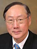
Dr. Michael L Chan - MD (Doctor of Medicine)
view sourceHospitals:
2250 Hayes St Suite #502, San Francisco, CA 94117
Michael K L Chan MD
1828 El Camino Real Suite 406, Burlingame, CA 94010
St. Mary's Medical Center
450 Stanyan Street, San Francisco, CA 94117
California Pacific Medical Center - California
3700 California Street, San Francisco, CA 94118
Chinese Hospital
845 Jackson Street, San Francisco, CA 94133
Michael K L Chan MD
1828 El Camino Real Suite 406, Burlingame, CA 94010
St. Mary's Medical Center
450 Stanyan Street, San Francisco, CA 94117
California Pacific Medical Center - California
3700 California Street, San Francisco, CA 94118
Chinese Hospital
845 Jackson Street, San Francisco, CA 94133
Philosophy:
caring, good listener, dedicated, intelligent, compassionate, committed, healing and reassuring.
Education:
Medical Schools
Creighton University School Of Medicine
Graduated: 1974
Creighton University School Of Medicine
Graduated: 1974

Dr. Michael Y Chan, San Francisco CA - DDS (Doctor of Dental Surgery)
view sourceSpecialties:
Oral & Maxillofacial Surgery
Address:
2001 Van Ness Ave Suite 401, San Francisco, CA 94109
(415)7766710 (Phone), (415)7762850 (Fax)
(415)7766710 (Phone), (415)7762850 (Fax)
Languages:
English

Dr. Michael C Chan - MD (Doctor of Medicine)
view sourceSpecialties:
Cardiology
Interventional Cardiology
Interventional Cardiology
Languages:
English
Spanish
Spanish
Education:
Medical School
Loma Linda University School Of Medicine
Graduated: 1974
Medical School
St Vincent Hospital
Graduated: 1992
Medical School
Oregon Health and Science University
Graduated: 1994
Medical School
University Hong Kong Hospital Princess Margaret Hospital
Graduated: 1994
Medical School
Stanford University
Graduated: 1998
Medical School
University Manitoba
Graduated: 1997

Michael Y. Chan
view sourceSpecialties:
Cardiovascular Disease
Work:
St Joseph Heritage Medical GroupSt Josephs Heritage Healthcare
1140 W Ln Veta Ave STE 430, Orange, CA 92868
(714)5435555 (phone), (714)5435585 (fax)
1140 W Ln Veta Ave STE 430, Orange, CA 92868
(714)5435555 (phone), (714)5435585 (fax)
Education:
Medical School
Stanford University School of Medicine
Graduated: 1997
Stanford University School of Medicine
Graduated: 1997
Procedures:
Angioplasty
Echocardiogram
Pacemaker and Defibrillator Procedures
Echocardiogram
Pacemaker and Defibrillator Procedures
Conditions:
Conduction Disorders
Ischemic Heart Disease
Valvular Heart Disease
Acute Myocardial Infarction (AMI)
Angina Pectoris
Ischemic Heart Disease
Valvular Heart Disease
Acute Myocardial Infarction (AMI)
Angina Pectoris
Languages:
English
Spanish
Spanish
Description:
Dr. Chan graduated from the Stanford University School of Medicine in 1997. He works in Orange, CA and specializes in Cardiovascular Disease. Dr. Chan is affiliated with Hoag Memorial Hospital Presbyterian, Saint Jude Medical Center and St Joseph Hospital Of Orange.

Michael W. Chan
view sourceSpecialties:
Cardiovascular Disease
Work:
Michael W Chan MD
98-1079 Moanalua Rd STE 655, Aiea, HI 96701
(808)6775585 (phone), (808)4863736 (fax)
98-1079 Moanalua Rd STE 655, Aiea, HI 96701
(808)6775585 (phone), (808)4863736 (fax)
Education:
Medical School
University of California, Irvine School of Medicine
Graduated: 1988
University of California, Irvine School of Medicine
Graduated: 1988
Procedures:
Angioplasty
Conditions:
Aortic Valvular Disease
Atrial Fibrillation and Atrial Flutter
Conduction Disorders
Heart Failure
Acute Myocardial Infarction (AMI)
Atrial Fibrillation and Atrial Flutter
Conduction Disorders
Heart Failure
Acute Myocardial Infarction (AMI)
Languages:
English
Description:
Dr. Chan graduated from the University of California, Irvine School of Medicine in 1988. He works in Aiea, HI and specializes in Cardiovascular Disease. Dr. Chan is affiliated with Pali Momi Medical Center.

Michael D. Chan
view sourceSpecialties:
Radiation Oncology
Work:
Wake Forest Baptist Health Radiation Oncology
1 Medical Ctr Blvd, Winston Salem, NC 27157
(336)7133600 (phone), (336)7136622 (fax)
1 Medical Ctr Blvd, Winston Salem, NC 27157
(336)7133600 (phone), (336)7136622 (fax)
Education:
Medical School
New York University School of Medicine
Graduated: 2003
New York University School of Medicine
Graduated: 2003
Conditions:
Anxiety Phobic Disorders
Malignant Neoplasm of Female Breast
Melanoma
Malignant Neoplasm of Female Breast
Melanoma
Languages:
Chinese
English
English
Description:
Dr. Chan graduated from the New York University School of Medicine in 2003. He works in Winston-Salem, NC and specializes in Radiation Oncology. Dr. Chan is affiliated with Wake Forest Baptist Health-Lexington Medical Center.

Michael Chan, San Francisco CA
view sourceSpecialties:
Marriage & Family Therapy
Address:
6221 Geary Blvd Suite 2, San Francisco, CA 94121
(415)4747310 (Phone)
(415)4747310 (Phone)
Languages:
English

Michael P. Chan
view sourceSpecialties:
Internal Medicine
Work:
Northeast Medical Group Hospitalist
20 York St STE CB-2041, New Haven, CT 06510
(203)6884748 (phone), (203)6884740 (fax)
20 York St STE CB-2041, New Haven, CT 06510
(203)6884748 (phone), (203)6884740 (fax)
Education:
Medical School
Rosalind Franklin University/ Chicago Medical School
Graduated: 2012
Rosalind Franklin University/ Chicago Medical School
Graduated: 2012
Languages:
English
Description:
Dr. Chan graduated from the Rosalind Franklin University/ Chicago Medical School in 2012. He works in New Haven, CT and specializes in Internal Medicine. Dr. Chan is affiliated with Yale New Haven Hospital.
Resumes

Michael Chan Sunnyvale, CA
view sourceWork:
CORDIS
Fremont, CA
2013 to 2014
Staff Operations Leader HERAEUS MEDICAL COMPONENTS, INC
White Bear Lake, MN
2011 to 2013
Senior Process Engineer ST. JUDE MEDICAL, INC
Minnetonka, MN
2010 to 2011
Advanced Process Development Engineer (Catheters) SCANLAN INTERNATIONAL, INC
Saint Paul, MN
2008 to 2010
Product Development Engineer DONATELLE PLASTICS, INC
New Brighton, MN
2005 to 2008
Project Engineer
Education:
University of St. Thomas, Opus College of Business
Minneapolis, MN
2012
MBA in Strategy & Operations University of Minnesota, Institute of Technology
Minneapolis, MN
2005
B.S. in Mechanical Engineering
Minneapolis, MN
2012
MBA in Strategy & Operations University of Minnesota, Institute of Technology
Minneapolis, MN
2005
B.S. in Mechanical Engineering

Michael Chan San Francisco, CA
view sourceWork:
Teamview Player Services, LLC
San Jose, CA
Mar 2010 to Jan 2013
Banker AT&T
San Francisco, CA
Dec 2008 to Feb 2010
Retail Sales Consultant Wells Fargo Bank
San Francisco, CA
Dec 2005 to Mar 2007
Bank Teller Houdini's Magic Shop
San Francisco, CA
Aug 2004 to Mar 2006
Assistant Manager/ Magician/ Cashier
San Jose, CA
Mar 2010 to Jan 2013
Banker AT&T
San Francisco, CA
Dec 2008 to Feb 2010
Retail Sales Consultant Wells Fargo Bank
San Francisco, CA
Dec 2005 to Mar 2007
Bank Teller Houdini's Magic Shop
San Francisco, CA
Aug 2004 to Mar 2006
Assistant Manager/ Magician/ Cashier
Education:
San Francisco State University
San Francisco, CA
Sep 2003 to Jun 2006
Business Finance City College of San Francisco
San Francisco, CA
Sep 2001 to Jun 2003
General Education
San Francisco, CA
Sep 2003 to Jun 2006
Business Finance City College of San Francisco
San Francisco, CA
Sep 2001 to Jun 2003
General Education

Michael Chan San Mateo, CA
view sourceWork:
Qualcomm Technologies Inc
Santa Clara, CA
Jun 2013 to Sep 2013
Modem Firmware Intern Life Technologies
Foster City, CA
Jun 2012 to Sep 2012
Embedded Systems Intern Motion Sensor Alarm Clock
Aug 2012 to Aug 2012 Elevator Controller
May 2012 to May 2012 Smetris
May 2011 to May 2011 Eagle Scout
Sep 2002 to Aug 2010
Santa Clara, CA
Jun 2013 to Sep 2013
Modem Firmware Intern Life Technologies
Foster City, CA
Jun 2012 to Sep 2012
Embedded Systems Intern Motion Sensor Alarm Clock
Aug 2012 to Aug 2012 Elevator Controller
May 2012 to May 2012 Smetris
May 2011 to May 2011 Eagle Scout
Sep 2002 to Aug 2010
Education:
UNIVERSITY OF CALIFORNIA
Los Angeles, CA
Sep 2010 to Mar 2011
Bachelor of Science in Electrical Engineering-Computer Engineering Option
Los Angeles, CA
Sep 2010 to Mar 2011
Bachelor of Science in Electrical Engineering-Computer Engineering Option

Michael Chan San Francisco, CA
view sourceWork:
Saratoga Star Aquatics
Sep 2010 to 2000
Assistant Manager Fremont Bank
Fremont, CA
Dec 2009 to Apr 2010
Customer Service Associate ASUS Computer International
Fremont, CA
Sep 2008 to Nov 2009
Accounting Assistant ABBYY USA Software House Inc
Fremont, CA
Jul 2007 to Sep 2008
Shipping Clerk / Technical Support
Sep 2010 to 2000
Assistant Manager Fremont Bank
Fremont, CA
Dec 2009 to Apr 2010
Customer Service Associate ASUS Computer International
Fremont, CA
Sep 2008 to Nov 2009
Accounting Assistant ABBYY USA Software House Inc
Fremont, CA
Jul 2007 to Sep 2008
Shipping Clerk / Technical Support
Education:
San Jose State University
Dec 2011
Bachelor of Science in Business Administration
Dec 2011
Bachelor of Science in Business Administration

Michael Chan Milpitas, CA
view sourceWork:
IBM
Oct 2012 to 2000
Graduate Materials Science Researcher eBay store
Jan 2012 to 2000
Owner of Business San Jose State University
Jan 2012 to 2000
Graduate Teaching Associate JP Research
Mountain View, CA
Jun 2012 to Aug 2012
Coder Certified Genetool
Milpitas, CA
Jan 2010 to Oct 2010
Service Engineer Omnica
Lake Forest, CA
Sep 2006 to Mar 2007
Senior Design Project University of California Irvine
Irvine, CA
Jun 2005 to Dec 2005
Stacker
Education:
San Jose State University
San Jose, CA
2011 to 2013
M.S. in Material Engineering De Anza College
Cupertino, CA
2009 to 2013
A.S. in Computer Aided Drafting University of California Irvine
Irvine, CA
2003 to 2008
B.S. in Biomedical Engineering Specialization: Biophotonics; Minor: Management
San Jose, CA
2011 to 2013
M.S. in Material Engineering De Anza College
Cupertino, CA
2009 to 2013
A.S. in Computer Aided Drafting University of California Irvine
Irvine, CA
2003 to 2008
B.S. in Biomedical Engineering Specialization: Biophotonics; Minor: Management
Plaxo

Michael Chan
view sourceSomerset House, Quarry Bay, Hong Kong

Chan Michael
view sourceSingaporeSymantec

Michael Chan
view sourceEL Sobrante, CA

Michael Chan
view sourceMelbourneManaging Director at AMG Group of Companies

Chan Michael
view sourceResorts World At Sentosa

Michael Chan
view sourceGlasgow, Scotland
Myspace
News

Hong Kong police respond with tear gas, water cannons as protesters mark new year with yet another mass demonstration
view source- We can try to push the movement to the next level and increase our efforts for a general strike, said Michael Chan, an organizer at the Catering and Hotel Industry Employees General Union, who was manning a booth encouraging people to sign up. We want to tell laborers that it is possible for them
- Date: Jan 01, 2020
- Category: Headlines
- Source: Google

Ontario Premier Wynne unveils massive midterm cabinet shuffle
view source- only of research, innovation and science. Other demotions include Michael Chan, who loses citizenship and immigration, retaining only international trade and Tracy MacCharles, who loses children and youth services to Michael Coteau but remains in cabinet as minister responsible for womens issues.
- Date: Jun 13, 2016
- Source: Google

Ontario minister Michael Chan defends China's human-rights record
view source- awa last week with his Canadian counterpart, Stphane Dion. [Mr. Wang] touched on the issue of human rights and his response led to commentary from all quarters, an unidentified scribe writes. A journalist interviewed Michael Chan about this, inviting him to share his views on the matter.y said. I dont think I have ever heard Michael Chan assert Canadas interests as against Chinese policy and Ive never heard him assert Canadian principles with respect to human rights as it relates to the PRC. So I think that undermines the Canadian position, which should be a balanced one.
- Date: Jun 08, 2016
- Source: Google

Pastor Rob Buckingham speaks after Bali Nine executions
view source- RB: [Andrews brother] Michael Chan put out a statement the other day and that really resonated with me. He asked Australians to remember Andrew Chan as a pastor rather than the kingpin. I will remember Andrew not as what he did just over a decade ago, but as the Andrew that we came to know and love
- Date: Apr 29, 2015
- Category: World
- Source: Google

Indonesian court agrees to hear challenge by Australians on death row
view source- "We've had a special day today," Michael Chan said as he announced the marriage after returning from a visit to the high-security Nusakambangan Island. "We've celebrated with some family and close friends.
- Date: Apr 27, 2015
- Source: Google

'Bali Nine' Convict Andrew Chan Marries in Indonesia Hours Before Possible ...
view source- "It's tough times but it's happy times at the same time," Michael Chan, Andrew's brother, told reporters outside the Nusakambangan island jail, where the executions will take place. "We just hope that the president somewhere will find some compassion and mercy for these two, this young couple so the
- Date: Apr 27, 2015
- Source: Google

Bali nine: Andrew Chan and fiancee reunite on execution island
view source- "Andrew was very happy to see some new faces today, especially Feby," Michael Chan told Fairfax Media after catching up with Febyanti and his family post-visit. "Just to be able to give his extended family hugs, and for them to pass on verbal messages of support to him has been very good and kept hi
- Date: Mar 11, 2015
- Category: World
- Source: Google

Andrew Chan's fiancee Febyanti Herewila joins visit to Bali nine execution island
view source- As Febyanti and Michael Chan frantically negotiated with prison officials, she was in tears. The bid to see Chan was futile, and he and Sukumaran left the prison in an armoured personnel carrier 30 minutes later.
- Date: Mar 10, 2015
- Category: World
- Source: Google

James Michael Chan
view source
Michael Vincent Chan
view source
Michael Vincent Chan
view source
Michael Chan
view source
Michael Chan Hian Seng
view source
Michael Dominguez Chan
view source
Michael Chan Chee Leg
view source
Michael Chan N Friends
view sourceGoogleplus
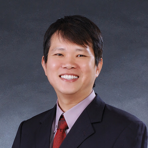
Michael Chan
Work:
Institute of Technical Education - Senior Lecturer (2013)
Punggol Primary School - Relief Teacher (2013-2013)
Global EduHub Pte Ltd - General Manager (International Office) (2012-2013)
China-Singapore International Education Services Ltd - General Manager, Support Services (2010-2012)
Republic of Singapore Navy - Chief Instructor (1988-1997)
Pei Hwa Presbyterian Primary School - Head of Pastoral Care and Pupil Welfare (1997-2002)
Dennis Wee Realty Pte Ltd - Marketing Associate (2002-2003)
Ten Talents Media Pte Ltd - Director (2003-2004)
Shanghai Singapore International School - Head of Primary School (2004-2010)
Education:
Singapore Polytechnic - Diploma in Electronics and Communications, Nanyang Technological University - Diploma in Education, University of Melbourne - Masters in Business Administration
Tagline:
A sinner knows best the grace and mercy of God.
Michael Chan
Lived:
So. San Francisco, CA
Saratoga CA
Hong Kong
Texas
Saratoga CA
Hong Kong
Texas
Work:
Legacy Through Giving Foundation - Helping Non-profits
Advanced Micro Devices
Fairchild Semiconductor
Texas Instruments
Raytheon Semiconductor
Gasonics International
America Printing
Advanced Micro Devices
Fairchild Semiconductor
Texas Instruments
Raytheon Semiconductor
Gasonics International
America Printing
Education:
San José State University, Wah Yan College, Kowloon, Raimondi College, Hong Kong
About:
Helped create Silicon Valley from 1967 when started to work in the semicondcutor engineering management arena. After 25 years in the high tech business, retired early and focus on community services ...
Bragging Rights:
Silicon Valley Pioneer, Who's Who of Inventors, Who's Who of Entrepreneur, Founder of MM Foundation, Founder of Legacy Through Giviing Foundation, Founder of Lions of Life
Michael Chan
Work:
Planning Center Online - Web Developer (2013)
Sonic Boom Wellness - UI Developer (2012-2013)
Miva Merchant - Web Developer (2011-2012)
Sonic Boom Wellness - UI Developer (2012-2013)
Miva Merchant - Web Developer (2011-2012)
Education:
Biola University - Organizational Leadership, MiraCosta College - Studio Recording, Sound Reinforcement, General
Relationship:
Married

Michael Chan
Work:
MPowa - IOS Software Engineer (2012)
WHSmith - Sales Assistant (2007-2008)
Future Platforms - Junior iOS Developer (2012-2012)
WHSmith - Sales Assistant (2007-2008)
Future Platforms - Junior iOS Developer (2012-2012)
Education:
King's College London - Computer Science
Tagline:
Hello :)
Michael Chan
Lived:
Milpitas, CA
Hong Kong
Guam
California
Hong Kong
Guam
California
Work:
Sony Computer Entertainment - Digital Operator (2010)
Education:
Notre Dame de Namur University - Software Engineering
Tagline:
Member since 07/11/2011
Bragging Rights:
Survived for 27 years
Michael Chan
Lived:
Palo Alto, California
Work:
Stanford University - Research Assistant
Education:
University of Michigan

Michael Chan
Work:
Étoile Consulting Group - Director and CEO (10)
Education:
London School of Economics - MSc (Econs) ADMIS, University of Hertfordshire - BSc (1st Class Hons) Applied Computing
Tagline:
An officer and a gentleman

Michael Chan
Work:
BDO International - Staff Accountant (2008)
Education:
University of Waterloo - Biotechnology/Accounting, University of Waterloo - Masters of Accounting
Classmates

Michael Chan
view sourceSchools:
Sugarloaf High School Campbellton NB 1977-1981
Community:
Sheila Theriault, Robert Murray

Michael Chan
view sourceSchools:
North High School Minneapolis MN 1994-1998
Community:
Rondeana Sandbeck

Michael Chan
view sourceSchools:
Fairfield High School Fairfield VA 1982-1986
Community:
William Clifton, Ruth Lilley

Michael Chan
view sourceSchools:
University of British Columbia - Political Science Vancouver Saudi Arabia 1995-1999
Community:
Joe Pearce

Michael Chan
view sourceSchools:
Manoah Steves Elementary School Richmond Saudi Arabia 1982-1986
Community:
Barry Kleven, Guy Hemphill, Sherry Bowerman

Michael Chan
view sourceSchools:
Mountain Pointe High School Phoenix AZ 1992-1996
Community:
Jennifer Zverina

Michael Chan
view sourceSchools:
Lord Kitchener Elementary School Vancouver Saudi Arabia 1996-1997
Community:
Ross Dunseith, John Raphael

Michael Chan
view sourceSchools:
Fairbanks High School Fairbanks AK 1980-1984
Community:
Terry Howe, Dick Steffe, Marlene Robb
Flickr
Youtube
Get Report for Michael N Chan from Newark, CA, age ~38


