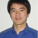
Yong He Jiang
age ~49
from San Francisco, CA
- Also known as:
-
- Yong H Jiang
- Yonghe H Jiang
- He Jiang Yonghe
Yong Jiang Phones & Addresses
- San Francisco, CA
- 90 Kilsyth Rd APT 6, Brighton, MA 02135
- Boston, MA
- Newton, MA
- Stopover, KY
- South San Francisco, CA
- Malden, MA
Medicine Doctors

Yong Mei Jiang
view sourceSpecialties:
Internal Medicine
Education:
Medical School
University of Colorado School of Medicine at Denver
Graduated: 2002
University of Colorado School of Medicine at Denver
Graduated: 2002
Conditions:
Acute Myocardial Infarction (AMI)
Acute Pancreatitis
Acute Renal Failure
Alcohol Dependence
Anemia
Acute Pancreatitis
Acute Renal Failure
Alcohol Dependence
Anemia
Description:
Dr. Jiang graduated from the University of Colorado School of Medicine at Denver in 2002. She works in Greenwood Village, CO and specializes in Internal Medicine. Dr. Jiang is affiliated with Kindred Hospital Aurora, Littleton Adventist Hospital and Sky Ridge Medical Center.
Us Patents
-
Network Interface With Double Data Rate And Delay Locked Loop
view source -
US Patent:6920552, Jul 19, 2005
-
Filed:Feb 27, 2002
-
Appl. No.:10/083291
-
Inventors:Jonathan Lin - Fremont CA, US
Yong Jiang - Fremont CA, US -
Assignee:Broadcom Corporation - Irvine CA
-
International Classification:G03F007/38
-
US Classification:713 1
-
Abstract:A network device is provided which includes a device input, at least one port, a frequency doubler, a data I/O device, and a programmable delay locked loop. The frequency doubler is coupled to the input and configured to receive an input signal and output an output signal having double the frequency of the input signal. The data I/O device is configured to output data based upon a reference clock signal. The programmable delay locked loop is coupled to the device input and configured to receive an input signal and to automatically output an output signal being a predetermined amount out of phase from the input signal. An external clock signal received at the device input is input to the frequency doubler. The output of the frequency doubler is input to the data I/O device as a reference clock. Data (e. g. , from internal device logic) is output from the data I/O device to the at least one port.
-
Network Interface Using Programmable Delay And Frequency Doubler
view source -
US Patent:6934866, Aug 23, 2005
-
Filed:Mar 18, 2002
-
Appl. No.:10/098337
-
Inventors:Jonathan Lin - Fremont CA, US
Yong Jiang - Fremont CA, US -
Assignee:Broadcom Corporaton - Irvine CA
-
International Classification:G06F001/12
-
US Classification:713401
-
Abstract:A network device includes an input, at least one port, a frequency doubler, a data I/O device, and a variable delay circuit. The input is for receiving an external clock signal. The frequency doubler is coupled to the input and configured to receive an input signal and output an output signal with a frequency double that of the input signal. The data I/O device is configured to output data to the at least one port based on a reference clock signal. The variable delay circuit is located between the data I/O device and at least one port. An external clock signal received at the input is input into the frequency doubler. The output signal of the frequency doubler is applied to the data I/O device as the reference clock signal, and the output data is delayed by the variable delay circuit.
-
Network Interface Using Programmable Delay And Frequency Doubler
view source -
US Patent:7024576, Apr 4, 2006
-
Filed:Jul 14, 2005
-
Appl. No.:11/180628
-
Inventors:Jonathan Lin - Fremont CA, US
Yong Jiang - Fremont CA, US -
Assignee:Broadcom Corporation - Irvine CA
-
International Classification:G04F 8/00
-
US Classification:713400
-
Abstract:A network device includes an input, at least one port, a frequency doubler, a data I/O device, and a variable delay circuit. The input is for receiving an external clock signal. The frequency doubler is coupled to the input and configured to receive an input signal and output an output signal with a frequency double that of the input signal. The data I/O device is configured to output data to the at least one port based on a reference clock signal. The variable delay circuit is located between the data I/O device and at least one port. An external clock signal received at the input is input into the frequency doubler. The output signal of the frequency doubler is applied to the data I/O device as the reference clock signal, and the output data is delayed by the variable delay circuit.
-
Network Interface With Double Data Rate And Delay Locked Loop
view source -
US Patent:7134010, Nov 7, 2006
-
Filed:Jun 10, 2005
-
Appl. No.:11/149182
-
Inventors:Jonathan Lin - Fremont CA, US
Yong Jiang - Fremont CA, US -
Assignee:Broadcom Corporation - Irvine CA
-
International Classification:G03F 7/38
-
US Classification:713 1
-
Abstract:A network device is provided which includes a device input, at least one port, a frequency doubler, a data I/O device, and a programmable delay locked loop. The frequency doubler is coupled to the input and configured to receive an input signal and output an output signal having double the frequency of the input signal. The data I/O device is configured to output data based upon a reference clock signal. The programmable delay locked loop is coupled to the device input and configured to receive an input signal and to automatically output an output signal being a predetermined amount out of phase from the input signal. An external clock signal received at the device input is input to the frequency doubler. The output of the frequency doubler is input to the data I/O device as a reference clock. Data (e. g. , from internal device logic) is output from the data I/O device to the at least one port.
-
Network Interface With Double Date Rate And Delay Locked Loop
view source -
US Patent:7308568, Dec 11, 2007
-
Filed:Oct 16, 2006
-
Appl. No.:11/580956
-
Inventors:Jonathan Lin - Fremont CA, US
Yong Jiang - Fremont CA, US -
Assignee:Broadcom Corporation - Irvine CA
-
International Classification:G03F 7/38
-
US Classification:713 1
-
Abstract:A network device is provided which includes a device input, at least one port, a frequency doubler, a data I/O device, and a programmable delay locked loop. The frequency doubler is coupled to the input and configured to receive an input signal and output an output signal having double the frequency of the input signal. The data I/O device is configured to output data based upon a reference clock signal. The programmable delay locked loop is coupled to the device input and configured to receive an input signal and to automatically output an output signal being a predetermined amount out of phase from the input signal. An external clock signal received at the device input is input to the frequency doubler. The output of the frequency doubler is input to the data I/O device as a reference clock. Data (e. g. , from internal device logic) is output from the data I/O device to the at least one port.
-
Method And Apparatus For Glitch-Free Control Of A Delay-Locked Loop In A Network Device
view source -
US Patent:7348820, Mar 25, 2008
-
Filed:Aug 29, 2006
-
Appl. No.:11/511309
-
Inventors:Yong H. Jiang - Fremont CA, US
-
Assignee:Broadcom Corporation - Irvine CA
-
International Classification:H03L 7/06
-
US Classification:327158, 327149
-
Abstract:A method of controlling a delay-locked loop (DLL) module is disclosed. The method includes the steps of receiving a clock signal, comparing the received clock signal with a reference clock signal to determine whether a required phase difference between the signals is within specified tolerances, producing a correction signal when the required phase difference between the received clock and reference clock signals is not within the specified tolerances, utilizing the correction signal to change a delay setting and forwarding the correction signal to slave DLL modules in communication with the DLL module. The comparing, producing, utilizing and forwarding steps are performed only after a period of time has elapsed from a prior incidence of the comparing, producing, utilizing and forwarding steps, where the period of time is sufficient to allow the DLL to settle and no extraneous results are produced.
Name / Title
Company / Classification
Phones & Addresses
President
MEI SHEN CORPORATION
Health and Allied Services, Nec, Nsk · Health/Allied Services · Nonclassifiable Establishments
Health and Allied Services, Nec, Nsk · Health/Allied Services · Nonclassifiable Establishments
2206 Irving St, San Francisco, CA 94122
1077 Powell St, San Francisco, CA 94108
1077 Powell St, San Francisco, CA 94108
Principal
Absolute Green Electric
Electrical Contractor
Electrical Contractor
1483 29 Ave, San Francisco, CA 94122
LEON AND ALAN, INCORPORATED
LEON AND ALAN, LLC
President
EVERGREEN QUALITY ENGINEERING, INC
3227 Foxboro Pl, San Jose, CA 95135
10440 S Anza Blvd, Cupertino, CA 95014
10440 S Anza Blvd, Cupertino, CA 95014
Resumes

Storage Engineer
view sourceLocation:
Orange, CA
Industry:
Internet
Work:
Western Digital Jul 2016 - Aug 2017
Principal Engineer
Facebook Jul 2016 - Aug 2017
Storage Engineer
Seagate Technology Sep 2012 - Feb 2013
Senior Engineer
The Hong Kong Polytechnic University Jan 2008 - Jan 2010
Research Assistant
Institute of Plasma Physics Chinese Academy of Sciences Jul 1, 2005 - Dec 1, 2007
Research Assistant
Principal Engineer
Facebook Jul 2016 - Aug 2017
Storage Engineer
Seagate Technology Sep 2012 - Feb 2013
Senior Engineer
The Hong Kong Polytechnic University Jan 2008 - Jan 2010
Research Assistant
Institute of Plasma Physics Chinese Academy of Sciences Jul 1, 2005 - Dec 1, 2007
Research Assistant
Education:
The Hong Kong Polytechnic University 2008 - 2010
Masters, Applied Physics, Philosophy University of Science and Technology of China 2001 - 2005
Bachelors, Applied Physics
Masters, Applied Physics, Philosophy University of Science and Technology of China 2001 - 2005
Bachelors, Applied Physics
Skills:
Failure Analysis
Design of Experiments
Hard Drives
Six Sigma
Testing
Data Analysis
Electronics
Semiconductors
Matlab
Product Development
Debugging
Storage
Materials Science
Firmware
Embedded Systems
Engineering Management
Minitab
Simulations
Project Management
Oscilloscope
Systems Engineering
Design of Experiments
Hard Drives
Six Sigma
Testing
Data Analysis
Electronics
Semiconductors
Matlab
Product Development
Debugging
Storage
Materials Science
Firmware
Embedded Systems
Engineering Management
Minitab
Simulations
Project Management
Oscilloscope
Systems Engineering
Languages:
Mandarin
English
English

Yong Jiang
view sourceLocation:
Boston, MA
Industry:
Arts And Crafts
Education:
Harvard University 2010 - 2011
Skills:
Microsoft Office
English
Research
Spss
English
Research
Spss

Engineer
view sourceLocation:
San Francisco, CA
Industry:
Electrical/Electronic Manufacturing
Work:
Brcm
Engineer
Nxp Semiconductors Aug 1998 - Apr 2000
Design Manager
Issi Aug 1995 - Aug 1998
Principal Design
Intel Corporation Jan 1990 - Jul 1995
Senior Design Engineer
Intel Corporation Jan 1990 - Jul 1995
Design Engineer
Engineer
Nxp Semiconductors Aug 1998 - Apr 2000
Design Manager
Issi Aug 1995 - Aug 1998
Principal Design
Intel Corporation Jan 1990 - Jul 1995
Senior Design Engineer
Intel Corporation Jan 1990 - Jul 1995
Design Engineer
Education:
University of California, Berkeley 1988 - 1990
Bachelors, Bachelor of Science
Bachelors, Bachelor of Science
Skills:
Semiconductors
Asic
Soc
Verilog
Ic
Embedded Systems
Debugging
Eda
Fpga
Circuit Design
Mixed Signal
Static Timing Analysis
Analog
Rtl Design
Vlsi
Application Specific Integrated Circuits
Asic
Soc
Verilog
Ic
Embedded Systems
Debugging
Eda
Fpga
Circuit Design
Mixed Signal
Static Timing Analysis
Analog
Rtl Design
Vlsi
Application Specific Integrated Circuits
Languages:
English

Sales Manager
view sourceLocation:
San Francisco, CA
Industry:
Chemicals
Work:
Albemarle Corporation
Sales Manager
Sales Manager

Yong Jiang
view sourceLocation:
338 Columbia St, Cambridge, MA 02141
Industry:
Retail
Work:
Staples
Senior Ecommerce Analyst, Staples.com Portfolio Performance
Senior Ecommerce Analyst, Staples.com Portfolio Performance
Skills:
Financial Analysis
Forecasting and Budgeting
Problem Solving
Analytics
Financial Planning and Analysis
Essbase
Hyperion Enterprise
Financial Modeling
Forecasting
Sales
Business Strategy
Finance
E Commerce
Forecasting and Budgeting
Problem Solving
Analytics
Financial Planning and Analysis
Essbase
Hyperion Enterprise
Financial Modeling
Forecasting
Sales
Business Strategy
Finance
E Commerce
Interests:
Children
Economic Empowerment
Environment
Education
Science and Technology
Animal Welfare
Arts and Culture
Health
Economic Empowerment
Environment
Education
Science and Technology
Animal Welfare
Arts and Culture
Health
Languages:
English
Mandarin
Mandarin

Yong Jiang
view source
Yong Jiang
view sourceYoutube
Flickr
Googleplus

Yong Jiang
Work:
AprexBio (10)

Yong Jiang
About:
不要做随波逐流的人!

Yong Jiang
About:
Love China and love my parents
Bragging Rights:
拿着清洁工的工资,干着工程师的活

Yong Jiang

Yong Jiang

Yong Jiang

Yong Jiang

Yong Jiang

Yong Jiang
view source
Yong Jiang
view source
Yong Jiang
view source
Yong Jiang
view source
Yong Han Jiang
view source
Yong Jiang
view source
Yong Jiang
view source
Yong Jiang
view sourceMyspace
Get Report for Yong He Jiang from San Francisco, CA, age ~49


