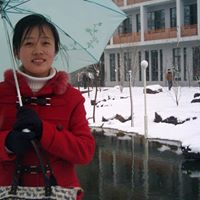
Jian Xin Zhao
age ~68
from San Diego, CA
- Also known as:
-
- Jian X Zhao
- Jianxin X Zhao
Jian Zhao Phones & Addresses
- San Diego, CA
- Edison, NJ
- Union, NJ
- San Bruno, CA
- Oxnard, CA
- San Francisco, CA
- Daly City, CA
Isbn (Books And Publications)

Optical Filter Design and Analysis: A Signal Processing Approach
view sourceAuthor
Jian H. Zhao
ISBN #
0471183733

Optical Filter Design and Analysis: A Signal Processing Approach
view sourceAuthor
Jian H. Zhao
ISBN #
0471213756

Stability Analysis and Modelling of Underground Excavations in Fractured Rocks
view sourceAuthor
Jian Zhao
ISBN #
0080430120
Medicine Doctors

Jian Zhao
view sourceSpecialties:
Anesthesiology
Work:
Mohawk Valley Anesthesia
178 Clizbe Ave, Amsterdam, NY 12010
(518)8435938 (phone), (518)8429633 (fax)
178 Clizbe Ave, Amsterdam, NY 12010
(518)8435938 (phone), (518)8429633 (fax)
Education:
Medical School
Xinjiang Med Coll, Urumqi City, Xinjiang Uygur Auto Reg, China
Graduated: 1983
Xinjiang Med Coll, Urumqi City, Xinjiang Uygur Auto Reg, China
Graduated: 1983
Languages:
Chinese
English
Korean
English
Korean
Description:
Dr. Zhao graduated from the Xinjiang Med Coll, Urumqi City, Xinjiang Uygur Auto Reg, China in 1983. He works in Amsterdam, NY and specializes in Anesthesiology. Dr. Zhao is affiliated with Saint Marys Healthcare.

Jian Zhao
view sourceSpecialties:
Anesthesiology
Pain Medicine
Pain Medicine
Education:
Xinjiang Medical University (1983)
Real Estate Brokers

Jian Ming Zhao, Daly City CA Agent
view sourceWork:
Realty World - Alliance
Daly City, CA
(415)3422844 (Phone)
License #01876035
Daly City, CA
(415)3422844 (Phone)
License #01876035
About:
As a full time professional real estate agent, I pride myself on offering superior personal service before, during and after your transaction. Knowledge, commitment, honesty, expertise and professionalism are the cornerstone of my business. Let me earn your trust, your business and most importantly your friendship. Don’t make another move without me. I guarantee you will see the difference quality service makes. I look forward to working with you!
Name / Title
Company / Classification
Phones & Addresses
President
Honey-B, Inc
Whol Groceries
Whol Groceries
2201 Clement St, San Francisco, CA 94121
739 Washington St, San Francisco, CA 94108
739 Washington St, San Francisco, CA 94108
President
Statlogic Group, LLC
Commercial Physical Research
Commercial Physical Research
22 Hancock Ct, Basking Ridge, NJ 07920
President
Rod Lifescience Inc
1070 Jackson St, Berkeley, CA 94706
President
U.S. ARTS EDUCATION CENTER (S.D.), INC
School/Educational Services
School/Educational Services
12812 Rancho Penasquitos Blvd #U, San Diego, CA 92129
(858)4847690
(858)4847690
President
FORTUNA MARBLE AND GRANITE, INC
Mfg Concrete Products Mfg Wood Kitchen Cabinets · Wood Kitchen Cabinet & Countertop Mfg
Mfg Concrete Products Mfg Wood Kitchen Cabinets · Wood Kitchen Cabinet & Countertop Mfg
1619 Whipple Rd, Hayward, CA 94544
(510)4751031, (510)4751819
(510)4751031, (510)4751819
COO, Principle, Chief Executive, CEO
jian hang zhao
1265 71 St APT 1FL, Brooklyn, NY 11228
(917)2028028
(917)2028028
Greenstar Micro Technologies LLC
Engineering Consulting and Foundry Servi · Business Services at Non-Commercial Site · Nonclassifiable Establishments
Engineering Consulting and Foundry Servi · Business Services at Non-Commercial Site · Nonclassifiable Establishments
10709 Matinal Cir, San Diego, CA 92127
10442 Duxbury Ln, San Diego, CA 92127
10442 Duxbury Ln, San Diego, CA 92127
BON BUFFET, INC
Us Patents
-
Field-Controlled High-Power Semiconductor Devices
view source -
US Patent:6423986, Jul 23, 2002
-
Filed:Dec 8, 2000
-
Appl. No.:09/719327
-
Inventors:Jian J. Zhao - North Brunswick NJ
-
Assignee:Rutgers, The State University - New Brunswick NJ
-
International Classification:H01L 2987
-
US Classification:257138, 257139, 257133, 257110, 257147, 257134
-
Abstract:Power semiconductor devices have a plurality of semiconductor layers of alternating p-type and n-type conductivity and top and bottom device surfaces. The top semiconductor layer forms a control layer ( ). A semiconductor layer junction, remote from both device surfaces, forms a blocking p-n junction ( ) capable of sustaining the applied device voltage. A top ohmic contact overlays a top conductive region ( ) extending from the top surface into the control layer ( ). A conductive tub region ( ), spaced apart from the top conductive region ( ), extends from the top surface at least through the control layer ( ). A field effect region ( ) is disposed in the control layer ( ) between the top conductive region ( ) and tub region ( ). A gate contact ( ) is formed over the field effect region ( ) causing the creation and interruption of a conductive channel ( ) between the top conductive region ( ) and conductive tub region ( ) so as to turn the device on and off.
-
Double-Gated Vertical Junction Field Effect Power Transistor
view source -
US Patent:6841812, Jan 11, 2005
-
Filed:Nov 7, 2002
-
Appl. No.:10/289907
-
Inventors:Jian Hui Zhao - North Brunswick NJ, US
-
Assignee:United Silicon Carbide, Inc. - New Brunswick NJ
-
International Classification:H01L 2980
H01L 2976
H01L 2994 -
US Classification:257256, 257329, 257341
-
Abstract:The present invention is a power semiconductor switch having a monolithically integrated low-voltage lateral junction field effect transistor (LJFET) controlling a high-voltage vertical junction field effect transistor (VJFET). The low-voltage LJFET conducting channel is double-gated by p+n junctions at opposite sides of the lateral channel. A buried p-type epitaxial layer forms one of the two p+n junction gates. A p+ region created by ion implantation serves as the p+ region for the second p+n junction gate. Both gates are electrically connected by a p+ tub implantation. The vertical channel of the vertical JFET is formed by converting part of the buried p-type epitaxial layer into n+ channel via n-type ion implantation.
-
Power Junction Field Effect Power Transistor With Highly Vertical Channel And Uniform Channel Opening
view source -
US Patent:7479672, Jan 20, 2009
-
Filed:Apr 9, 2007
-
Appl. No.:11/784613
-
Inventors:Jian H. Zhao - North Brunswick NJ, US
-
Assignee:Rutgers, The State University - New Brunswick NJ
-
International Classification:H01L 29/80
-
US Classification:257256, 257134, 257135, 257272, 257192, 257195, 257274, 257E27148
-
Abstract:A semiconductor vertical junction field effect power transistor formed by a semiconductor structure having top and bottom surfaces and including a plurality of semiconductor layers with predetermined doping concentrations and thicknesses and comprising at least a bottom layer as drain layer, a middle layer as blocking and channel layer, a top layer as source layer. A plurality of laterally spaced U-shaped trenches with highly vertical side walls defines a plurality of laterally spaced mesas. The mesas are surrounded on the four sides by U-shaped semiconductor regions having conductivity type opposite to that of the mesas forming U-shaped pn junctions and defining a plurality of laterally spaced long and vertical channels with a highly uniform channel opening dimension. A source contact is formed on the top source layer and a drain contact is formed on the bottom drain layer. A gate contact is formed on the bottom of the U-shaped trenches for the purpose of creating and interrupting the vertical channels so as to turn on and turn off the transistor.
-
Vertical Junction Field Effect Power Transistor
view source -
US Patent:20050067630, Mar 31, 2005
-
Filed:Sep 25, 2003
-
Appl. No.:10/671233
-
Inventors:Jian Zhao - North Brunswick NJ, US
-
International Classification:H01L029/74
H01L031/111 -
US Classification:257134000, 257135000, 257136000
-
Abstract:A semiconductor vertical junction field effect power transistor formed by a semiconductor structure having top and bottom surfaces and including a plurality of semiconductor layers with predetermined doping concentrations and thicknesses and comprising at least a bottom layer as drain layer, a middle layer as blocking and channel layer, a top layer as source layer. A plurality of laterally spaced U-shaped trenches with highly vertical side walls defines a plurality of laterally spaced mesas. The mesas are surrounded on the four sides by U-shaped semiconductor regions having conductivity type opposite to that of the mesas forming U-shaped pn junctions and defining a plurality of laterally spaced long and vertical channels with a highly uniform channel opening dimension. A source contact is formed on the top source layer and a drain contact is formed on the bottom drain layer. A gate contact is formed on the bottom of the U-shaped trenches for the purpose of creating and interrupting the vertical channels so as to turn on and turn off the transistor.
-
Power Junction Field Effect Power Transistor With Highly Vertical Channel And Uniform Channel Opening
view source -
US Patent:20100148224, Jun 17, 2010
-
Filed:Jan 19, 2009
-
Appl. No.:12/355978
-
Inventors:Jian H. Zhao - North Brunswick NJ, US
-
Assignee:Rutgers, The State University of New Jersey - New Brunswick NJ
-
International Classification:H01L 29/80
-
US Classification:257263, 257E2931
-
Abstract:A semiconductor vertical junction field effect power transistor formed by a semiconductor structure having top and bottom surfaces and including a plurality of semiconductor layers with predetermined doping concentrations and thicknesses and comprising at least a bottom layer as drain layer, a middle layer as blocking and channel layer, a top layer as source layer. A plurality of laterally spaced U-shaped trenches with highly vertical side walls defines a plurality of laterally spaced mesas. The mesas are surrounded on the four sides by U-shaped semiconductor regions having conductivity type opposite to that of the mesas forming U-shaped pn junctions and defining a plurality of laterally spaced long and vertical channels with a highly uniform channel opening dimension. A source contact is formed on the top source layer and a drain contact is formed on the bottom drain layer. A gate contact is formed on the bottom of the U-shaped trenches for the purpose of creating and interrupting the vertical channels so as to turn on and turn off the transistor.
-
Watermark Extraction And Content Screening In A Networked Environment
view source -
US Patent:20120072729, Mar 22, 2012
-
Filed:Apr 5, 2011
-
Appl. No.:13/080593
-
Inventors:Joseph M. Winograd - San Diego CA, US
Rade Petrovic - San Diego CA, US
Jian Zhao - Montrose CA, US -
International Classification:G06F 21/24
-
US Classification:713176
-
Abstract:Methods, devices, and computer program products facilitate the application of a content use policy based on watermarks that are embedded in a content. Watermark extraction and content screening operations, which can include the application of content usage enforcement actions, may be organized such that some or all of the operations can be conducted at different times by different devices. The watermark extraction results can be stored in a secure location and accessed by other devices at different times. These operations can be conducted by one or more trusted devices that reside in a home network. The home network can also include a gateway device that can coordinate the operations of the various network devices and/or delegate the various watermark extraction and content screening operations.
-
Context Access Management Using Watermark Extraction Information
view source -
US Patent:20120072730, Mar 22, 2012
-
Filed:Apr 5, 2011
-
Appl. No.:13/080598
-
Inventors:Joseph M. Winograd - San Diego CA, US
Rade Petrovic - San Diego CA, US
Jian Zhao - Montrose CA, US -
International Classification:H04L 9/32
-
US Classification:713176
-
Abstract:Methods, devices, and computer program products facilitate the application of a content use policy based on watermarks that are embedded in a content. Watermark extraction and content screening operations, which can include the application of content usage enforcement actions, may be organized such that some or all of the operations can be conducted at different times by different devices. These operations can be conducted by one or more trusted devices that reside in a networked environment. Real-time access to a content can also be facilitated by utilizing existing watermark extraction records. To facilitate real-time access to the content, the extraction records may contain segmented authentication information that correspond to particular segments of the content that is being accessed. Additionally, or alternatively, new watermark extraction operations can be conducted in real-time to produce new watermark extraction records.
-
Secure And Efficient Content Screening In A Networked Environment
view source -
US Patent:20120072731, Mar 22, 2012
-
Filed:Apr 5, 2011
-
Appl. No.:13/080605
-
Inventors:Joseph M. Winograd - San Diego CA, US
Rade Petrovic - San Diego CA, US
Jian Zhao - Montrose CA, US -
International Classification:G06F 21/24
-
US Classification:713176
-
Abstract:Methods, devices, and computer program products facilitate the application of a content use policy based on watermarks that are embedded in a content. Watermark extraction and content screening operations, which can include the application of content usage enforcement actions, may be organized such that some or all of the operations can be conducted at different times by different devices. These operations can be conducted by one or more trusted devices that reside in a networked environment. The authenticity of various devices can be verified through the exchange of certificates that can further enable such devices to ascertain capabilities of one another. Based on the ascertained capabilities, an operational configuration for conducting watermark extraction and content screening can be determined.
Resumes

Phd Candidate & Graduate Assistant At Fordham University
view sourcePosition:
PhD Candidate at Fordham University
Location:
Greater New York City Area
Industry:
Higher Education
Work:
Fordham University - Bronx, NY since Sep 2009
PhD Candidate
PhD Candidate
Languages:
English
Chinese
Chinese

Director, Chemistry
view sourceLocation:
3678 Fallon Cir, San Diego, CA 92130
Industry:
Biotechnology
Work:
Crinetics Pharmaceuticals
Director, Chemistry
Pacific World Discovery Dec 2010 - Jul 2012
Senior Scientist
The Scripps Research Institute Aug 2009 - Nov 2010
Research Associate
Texas A&M University Apr 2007 - Jun 2009
Postdoctoral Research Associate
Director, Chemistry
Pacific World Discovery Dec 2010 - Jul 2012
Senior Scientist
The Scripps Research Institute Aug 2009 - Nov 2010
Research Associate
Texas A&M University Apr 2007 - Jun 2009
Postdoctoral Research Associate
Education:
Iowa State University Jan 1, 2001 - Dec 31, 2007
Doctorates, Doctor of Philosophy, Philosophy, Organic Chemistry Xiamen University Jan 1, 1994 - 2001
Bachelors, Bachelor of Science, Chemistry
Doctorates, Doctor of Philosophy, Philosophy, Organic Chemistry Xiamen University Jan 1, 1994 - 2001
Bachelors, Bachelor of Science, Chemistry
Skills:
Organic Synthesis
Nmr
Organic Chemistry
Drug Discovery
Drug Design
Lc Ms
Organometallic Chemistry
Nmr Spectroscopy
Purification
Hplc
Mass Spectrometry
Catalysis
Chemistry
Nmr
Organic Chemistry
Drug Discovery
Drug Design
Lc Ms
Organometallic Chemistry
Nmr Spectroscopy
Purification
Hplc
Mass Spectrometry
Catalysis
Chemistry
Languages:
English

Staff Architect
view sourceLocation:
16545 Newcomb St, San Diego, CA
Industry:
Semiconductors
Work:
Asml Feb 2017 - Feb 2018
Senior Architect
Asml Feb 2017 - Feb 2018
Staff Architect
Asml Jun 2014 - Jan 2017
Mdo and Project Leader
Asml 2011 - Jun 2014
Senior Scientist
Uc Santa Barbara Jan 2010 - Sep 2011
Senior Development Engineer
Senior Architect
Asml Feb 2017 - Feb 2018
Staff Architect
Asml Jun 2014 - Jan 2017
Mdo and Project Leader
Asml 2011 - Jun 2014
Senior Scientist
Uc Santa Barbara Jan 2010 - Sep 2011
Senior Development Engineer
Education:
Uc Santa Barbara 2000 - 2005
Doctorates, Doctor of Philosophy, Mechanical Engineering Uc Santa Barbara 2001 - 2003
Master of Science, Masters, Electrical Engineering Tsinghua University 1997 - 2000
Master of Science, Masters, Mechanical Engineering Tsinghua University 1992 - 1997
Bachelors, Bachelor of Science, Mechanical Engineering
Languages:
English
Certifications:
Six Sigma Green Belt (Cssgb)
Systems Engineering Certificate Courses (System Requirements Analysis, System Engineering Management, Introduction To System Thinking, Work Team Concepts and Skills, Hardware and Software Integration, Engineering Project Management)
Systems Engineering Certificate Courses (System Requirements Analysis, System Engineering Management, Introduction To System Thinking, Work Team Concepts and Skills, Hardware and Software Integration, Engineering Project Management)

Jian Zhao
view source
Jian Zhao
view source
Jian Zhao
view sourceLocation:
United States

Prof At Rutgers University
view sourcePosition:
Prof at Rutgers University
Location:
Greater New York City Area
Industry:
Higher Education
Work:
Rutgers University
Prof
Prof

Jian Zhao
view sourceLocation:
United States
Myspace
Youtube

Lu Jian Zhao
view source
Jian Zhao
view source
Jian Zhao
view source
Jian Wei Zhao
view source
Zhao Jian
view source
Jian Zhao
view source
Jian Zhao
view source
Jian Zhao
view sourceGoogleplus

Jian Zhao
Work:
Microsoft Research - Research Intern (2011-2011)
Education:
University of Toronto - Computer science

Jian Zhao
Work:
Jining
Education:
Xiamen university

Jian Zhao
Education:
Donvale Christian Collage

Jian Zhao
Tagline:
Sunshine! Optimistic! Happy!~~~Every cloud has a silver lining…

Jian “Robin” Zhao

Jian Zhao

Jian Zhao

Jian Zhao
Classmates

Jian Zhao
view sourceSchools:
Jinan University Guangzhou China 1991-1995

Jian Bin Zhao
view sourceSchools:
Timothy Eaton Business & Technical Institute Scarborough Morocco 1994-1998
Community:
Grace Barkwell, Dave Pringle, Shannon Savage, Sandra Theriault

Jinan University, Guangzhou
view sourceGraduates:
Yangchun Wang (1985-1989),
Jian Zhao (1991-1995),
Yu Huang (1996-2000)
Jian Zhao (1991-1995),
Yu Huang (1996-2000)

Morningside College, Siou...
view sourceGraduates:
Jian Zhao (1992-1994),
Deanna Stiegelmeyer (1956-1958),
Lorenzo Plyler (1963-1967)
Deanna Stiegelmeyer (1956-1958),
Lorenzo Plyler (1963-1967)

Timothy Eaton Business &a...
view sourceGraduates:
Jian Bin Zhao (1994-1998),
roberta Zelasko (1977-1981),
Dan Skelhorn (1972-1976),
Nicholas Prato (1993-1997),
John Lever (1980-1984)
roberta Zelasko (1977-1981),
Dan Skelhorn (1972-1976),
Nicholas Prato (1993-1997),
John Lever (1980-1984)
Get Report for Jian Xin Zhao from San Diego, CA, age ~68


