Anthony J Mccarthy
age ~35
from Merced, CA
Anthony Mccarthy Phones & Addresses
- Merced, CA
- Oakland, CA
Us Patents
-
Electroless Epitaxial Etching For Semiconductor Applications
view source -
US Patent:6346461, Feb 12, 2002
-
Filed:May 15, 2000
-
Appl. No.:09/570888
-
Inventors:Anthony M. McCarthy - Menlo Park CA
-
Assignee:The Regents of the University of California - Oakland CA
-
International Classification:H01L 2120
-
US Classification:438479, 438667, 438483
-
Abstract:A method for fabricating thin-film single-crystal silicon on insulator substrates using electroless etching for achieving efficient etch stopping on epitaxial silicon substrates. Microelectric circuits and devices are prepared on epitaxial silicon wafers in a standard fabrication facility. The wafers are bonded to a holding substrate. The silicon bulk is removed using electroless etching leaving the circuit contained within the epitaxial layer remaining on the holding substrate. A photolithographic operation is then performed to define streets and wire bond pad areas for electrical access to the circuit.
-
Silicon On Insulator Self-Aligned Transistors
view source -
US Patent:6649977, Nov 18, 2003
-
Filed:Sep 11, 1995
-
Appl. No.:08/526339
-
Inventors:Anthony M. McCarthy - Menlo Park CA
-
Assignee:The Regents of the University of California - Oakland CA
-
International Classification:H01L 2701
-
US Classification:257347, 257 67
-
Abstract:A method for fabricating thin-film single-crystal silicon-on-insulator (SOI) self-aligned transistors. Standard processing of silicon substrates is used to fabricate the transistors. Physical spaces, between the source and gate, and the drain and gate, introduced by etching the polysilicon gate material, are used to provide connecting implants (bridges) which allow the transistor to perform normally. After completion of the silicon substrate processing, the silicon wafer is bonded to an insulator (glass) substrate, and the silicon substrate is removed leaving the transistors on the insulator (glass) substrate. Transistors fabricated by this method may be utilized, for example, in flat panel displays, etc.
-
Method For Fabricating Transistors Using Crystalline Silicon Devices On Glass
view source -
US Patent:56630786, Sep 2, 1997
-
Filed:Jan 17, 1995
-
Appl. No.:8/373716
-
Inventors:Anthony M. McCarthy - Menlo Park CA
-
Assignee:Regents of the University of California - Oakland CA
-
International Classification:H01L 21786
-
US Classification:438157
-
Abstract:A method for fabricating transistors using single-crystal silicon devices on glass. This method overcomes the potential damage that may be caused to the device during high voltage bonding and employs a metal layer which may be incorporated as part of the transistor. This is accomplished such that when the bonding of the silicon wafer or substrate to the glass substrate is performed, the voltage and current pass through areas where transistors will not be fabricated. After removal of the silicon substrate, further metal may be deposited to form electrical contact or add functionality to the devices. By this method both single and gate-all-around devices may be formed.
-
Process For Protecting Bonded Components From Plating Shorts
view source -
US Patent:60514930, Apr 18, 2000
-
Filed:Oct 14, 1994
-
Appl. No.:8/323410
-
Inventors:Lisa A. Tarte - Livermore CA
Wayne L. Bonde - Pleasanton CA
Paul G. Carey - Mountain View CA
Robert J. Contolini - Pleasanton CA
Anthony M. McCarthy - Menlo Park CA -
Assignee:The Regents of the University of California - Oakland CA
-
International Classification:H01L 2144
-
US Classification:438662
-
Abstract:A method which protects the region between a component and the substrate onto which the components is bonded using an electrically insulating fillet of photoresist. The fillet protects the regions from subsequent plating with metal and therefore shorting the plated conductors which run down the sides of the component and onto the substrate.
-
Transistors Using Crystalline Silicon Devices On Glass
view source -
US Patent:54142768, May 9, 1995
-
Filed:Oct 18, 1993
-
Appl. No.:8/137402
-
Inventors:Anthony M. McCarthy - Menlo Park CA
-
Assignee:The Regents of the University of California
-
International Classification:H01L 2904
H01L 2978 -
US Classification:257 57
-
Abstract:A method for fabricating transistors using single-crystal silicon devices on glass. This method overcomes the potential damage that may be caused to the device during high voltage bonding and employs a metal layer which may be incorporated as part of the transistor. This is accomplished such that when the bonding of the silicon wafer or substrate to the glass substrate is performed, the voltage and current pass through areas where transistors will not be fabricated. After removal of the silicon substrate, further metal may be deposited to form electrical contact or add functionality to the devices. By this method both single and gate-all-around devices may be formed.
-
Silicon On Insulator With Active Buried Regions
view source -
US Patent:54880122, Jan 30, 1996
-
Filed:Oct 18, 1993
-
Appl. No.:8/137412
-
Inventors:Anthony M. McCarthy - Menlo Park CA
-
Assignee:The Regents of the University of California - Oakland CA
-
International Classification:H01L 2176
-
US Classification:437 62
-
Abstract:A method for forming patterned buried components, such as collectors, sources and drains, in silicon-on-insulator (SOI) devices. The method is carried out by epitaxially growing a suitable sequence of single or multiple etch stop layers ending with a thin silicon layer on a silicon substrate, masking the silicon such that the desired pattern is exposed, introducing dopant and activating in the thin silicon layer to form doped regions. Then, bonding the silicon layer to an insulator substrate, and removing the silicon substrate. The method additionally involves forming electrical contact regions in the thin silicon layer for the buried collectors.
-
Silicon On Insulator Achieved Using Electrochemical Etching
view source -
US Patent:56747586, Oct 7, 1997
-
Filed:Jun 6, 1995
-
Appl. No.:8/484062
-
Inventors:Anthony M. McCarthy - Menlo Park CA
-
Assignee:Regents of the University of California - Oakland CA
-
International Classification:H01L 2184
H01L 213063 -
US Classification:437 21
-
Abstract:Bulk crystalline silicon wafers are transferred after the completion of circuit fabrication to form thin films of crystalline circuitry on almost any support, such as metal, semiconductor, plastic, polymer, glass, wood, and paper. In particular, this technique is suitable to form silicon-on-insulator (SOI) wafers, whereby the devices and circuits formed exhibit superior performance after transfer due to the removal of the silicon substrate. The added cost of the transfer process to conventional silicon fabrication is insignificant. No epitaxial, lift-off, release or buried oxide layers are needed to perform the transfer of single or multiple wafers onto support members. The transfer process may be performed at temperatures of 50. degree. C. or less, permits transparency around the circuits and does not require post-transfer patterning. Consequently, the technique opens up new avenues for the use of integrated circuit devices in high-brightness, high-resolution video-speed color displays, reduced-thickness increased-flexibility intelligent cards, flexible electronics on ultrathin support members, adhesive electronics, touch screen electronics, items requiring low weight materials, smart cards, intelligent keys for encryption systems, toys, large area circuits, flexible supports, and other applications.
-
Silicon On Insulator With Active Buried Regions
view source -
US Patent:57604436, Jun 2, 1998
-
Filed:Oct 23, 1995
-
Appl. No.:8/547080
-
Inventors:Anthony M. McCarthy - Menlo Park CA
-
Assignee:Regents of the University of California - Oakland CA
-
International Classification:H01L 2176
-
US Classification:257347
-
Abstract:A method for forming patterned buried components, such as collectors, sources and drains, in silicon-on-insulator (SOI) devices. The method is carried out by epitaxially growing a suitable sequence of single or multiple etch stop layers ending with a thin silicon layer on a silicon substrate, masking the silicon such that the desired pattern is exposed, introducing dopant and activating in the thin silicon layer to form doped regions. Then, bonding the silicon layer to an insulator substrate, and removing the silicon substrate. The method additionally involves forming electrical contact regions in the thin silicon layer for the buried collectors.
Resumes

Mental Health Worker
view sourceLocation:
Merced, CA
Industry:
Mental Health Care
Work:
Merced County Mental Health
Mental Health Worker
Learning Arts
Behavior Technician
Mental Health Worker
Learning Arts
Behavior Technician

Anthony Amonu Mccarthy
view sourceWork:
Tj Maxx Mar 2011 - Feb 2013
Back Up Lead
Back Up Lead
Education:
University of Cape Coast 2005 - 2008

Anthony Mccarthy
view source
Anthony Mccarthy
view sourceLocation:
United States
Name / Title
Company / Classification
Phones & Addresses
Sun Valley Electric Ltd
Electric Contractors
Electric Contractors
109 2303 Leckie Rd, Kelowna, BC V1X 6Y5
(250)8604402, (250)8614843
(250)8604402, (250)8614843
President
THE PENINSULA FOUNDATION
Civic/Social Association
Civic/Social Association
770 S Windsor Blvd, Los Angeles, CA 90005
765 14 Ave, San Francisco, CA 94118
765 14 Ave, San Francisco, CA 94118
Sun Valley Electric Ltd
Electric Contractors
Electric Contractors
(250)8604402, (250)8614843
President
Menlough Study Center
Individual & Family Services · School/Educational Services
Individual & Family Services · School/Educational Services
1160 Santa Cruz Ave, Menlo Park, CA 94025
(650)3271675
(650)3271675
Myspace

Anthony McCarthy
view source
Anthony McCarthy
view sourceLocality:
Miami gardens/Brooklyn New York, Florida
Gender:
Male
Birthday:
1947
Flickr

Anthony J Mccarthy
view source
Anthony McCarthy
view source
Anthony McCarthy
view source
Anthony McCarthy
view source
Anthony Joseph Mccarthy
view source
Anthony David McCarthy
view source
Anthony McCarthy
view source
Anthony James McCarthy
view sourcePlaxo

Anthony McCarthy
view source
Anthony McCarthy
view sourceBelair, Luxembourg
Classmates

Anthony McCarthy
view sourceSchools:
Brother Rice High School St. John's Peru 1984-1988
Community:
Edward Bursey, Sheila Phillips, Bernice Hawco

Anthony McCarthy
view sourceSchools:
Central Elementary School Imperial Beach CA 1963-1969
Community:
Steve Sadler, Tonya Hale

Anthony McCarthy
view sourceSchools:
Arlington Elementary School Poughkeepsie NY 1958-1961, Krieger Elementary School Poughkeepsie NY 1959-1964, Forbus Junior High School Poughkeepsie NY 1965-1968
Community:
Mary Nye

Anthony McCarthy
view sourceSchools:
Pacific Lutheran Univesity Tacoma WA 2003-2007

Anthony McCarthy | Sarato...
view source
Anthony McCarthy | Martin...
view source
Krieger Elementary School...
view sourceGraduates:
Albert Lintel Jr (1936-1944),
Anthony McCarthy (1959-1964),
Nanci Gelb (1962-1968),
Quineisha Norwood (1995-2000)
Anthony McCarthy (1959-1964),
Nanci Gelb (1962-1968),
Quineisha Norwood (1995-2000)
Googleplus

Anthony Mccarthy
Work:
Everton Park Library - Trainee (2009)
Education:
Bracken Ridge State Highschool

Anthony Mccarthy

Anthony Mccarthy

Anthony Mccarthy

Anthony Mccarthy

Anthony Mccarthy
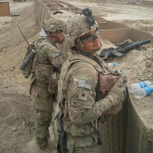
Anthony Mccarthy
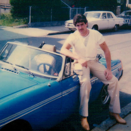
Anthony Mccarthy
Youtube
Get Report for Anthony J Mccarthy from Merced, CA, age ~35


