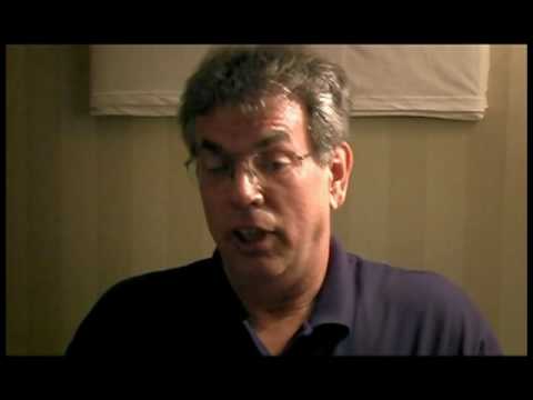
Frank J Evans
age ~73
from Corinth, MS
- Also known as:
-
- Frank A Evans
- Frank Addison Evans
- Frank N Evans
- Frank R Evans
- Jr Frank Evans
- Frank Evansjr
- Evans Franka
Frank Evans Phones & Addresses
- Corinth, MS
- Phoenix, AZ
- 418 Guyan St, Logan, WV 25601 • (304)7522773
- Portland, OR
- Gilbert, AZ
- Queen Creek, AZ
- Lexington, KY
- Roswell, GA
- Maricopa, AZ
Us Patents
-
Integrated Alignment And Calibration Of Optical System
view source -
US Patent:6678058, Jan 13, 2004
-
Filed:Oct 24, 2001
-
Appl. No.:10/039249
-
Inventors:Leo B. Baldwin - Beaverton OR
Frank G. Evans - Dundee OR -
Assignee:Electro Scientific Industries, Inc. - Portland OR
-
International Classification:G01B 1124
-
US Classification:356609, 356620, 356401
-
Abstract:A calibration system within an optical inspection apparatus comprising a sensor, lens, fiducials, and a CPU. The CPU is configured to receive information from the sensor relating to the fiducial coordinate system and the sensor coordinate system, and the fiducials are used to determine a physical relationship between the sensor coordinates and fiducial coordinates. The calibration system has a means for calibrating the inspection system and measuring critical dimensions of an object in an accurate manner on-the-fly without additional set-up or manual calibration of the system.
-
Semiconductor Structure Processing Using Multiple Laser Beam Spots Spaced On-Axis With Cross-Axis Offset
view source -
US Patent:7425471, Sep 16, 2008
-
Filed:Feb 4, 2005
-
Appl. No.:11/051958
-
Inventors:Kelly J. Bruland - Portland OR, US
Brian W. Baird - Oregon City OR, US
Ho Wai Lo - Portland OR, US
Stephen N. Swaringen - Rockwall TX, US
Frank G. Evans - Dundee OR, US -
Assignee:Electro Scientific Industries, Inc. - Portland OR
-
International Classification:H01L 21/82
-
US Classification:438130, 438 13, 21912168
-
Abstract:Methods and systems selectively irradiate structures on or within a semiconductor substrate using a plurality of laser beams. The structures are arranged in a row extending in a generally lengthwise direction. The method generates a first laser beam that propagates along a first laser beam axis that intersects the semiconductor substrate and a second laser beam that propagates along a second laser beam axis that intersects the semiconductor substrate. The method directs the first and second laser beams onto distinct first and second structures in the row. The second spot is offset from the first spot by some amount in a direction perpendicular to the lengthwise direction of the row. The method moves the first and second laser beam axes relative to the semiconductor substrate along the row substantially in unison in a direction substantially parallel to the lengthwise direction of the row.
-
Semiconductor Structure Processing Using Multiple Laser Beam Spots
view source -
US Patent:7923306, Apr 12, 2011
-
Filed:Feb 4, 2005
-
Appl. No.:11/052000
-
Inventors:Kelly J. Bruland - Portland OR, US
Brian W. Baird - Oregon City OR, US
Ho Wai Lo - Portland OR, US
Stephen N. Swaringen - Rockwall TX, US
Frank G. Evans - Dundee OR, US -
Assignee:Electro Scientific Industries, Inc. - Portland OR
-
International Classification:H01L 21/00
B23K 26/00 -
US Classification:438132, 21912176
-
Abstract:Methods and systems selectively irradiate structures on or within a semiconductor substrate using a plurality of pulsed laser beams. The structures are arranged in a row extending in a generally lengthwise direction. The method generates a first pulsed laser beam that propagates along a first laser beam axis that intersects the semiconductor substrate and a second pulsed laser beam that propagates along a second laser beam axis that intersects the semiconductor substrate. The method directs respective first and second pulses from the first and second pulsed laser beams onto distinct first and second structures in the row. The method moves the first and second laser beam axes relative to the semiconductor substrate substantially in unison in a direction substantially parallel to the lengthwise direction of the row.
-
Semiconductor Structure Processing Using Multiple Laser Beam Spots Spaced On-Axis On Non-Adjacent Structures
view source -
US Patent:7935941, May 3, 2011
-
Filed:Feb 4, 2005
-
Appl. No.:11/051263
-
Inventors:Kelly J. Bruland - Portland OR, US
Brian W. Baird - Oregon City OR, US
Ho Wai Lo - Portland OR, US
Frank G. Evans - Dundee OR, US -
Assignee:Electro Scientific Industries, Inc. - Portland OR
-
International Classification:B23K 26/08
B23K 26/38 -
US Classification:2504922, 25049222, 21912168, 21912169
-
Abstract:Methods and systems selectively irradiate structures on or within a semiconductor substrate using a plurality of laser beams. The structures are arranged in a row extending in a generally lengthwise direction. The method generates a first laser beam that propagates along a first laser beam axis that intersects the semiconductor substrate and a second laser beam that propagates along a second laser beam axis that intersects the semiconductor substrate. The method directs the first and second laser beams onto non-adjacent first and second structures in the row. The method moves the first and second laser beam axes relative to the semiconductor substrate along the row substantially in unison in a direction substantially parallel to the lengthwise direction of the row.
-
Semiconductor Structure Processing Using Multiple Laser Beam Spots Spaced On-Axis Delivered Simultaneously
view source -
US Patent:8148211, Apr 3, 2012
-
Filed:Feb 4, 2005
-
Appl. No.:11/051500
-
Inventors:Kelly J. Bruland - Portland OR, US
Brian W. Baird - Oregon City OR, US
Ho Wai Lo - Portland OR, US
Stephen N. Swaringen - Rockwall TX, US
Frank G. Evans - Dundee OR, US -
Assignee:Electro Scientific Industries, Inc. - Portland OR
-
International Classification:H01L 21/77
B23K 26/02
B23K 26/06
B23K 26/08
B23K 26/40 -
US Classification:438131, 438132, 219 68, 219162
-
Abstract:Methods and systems selectively irradiate structures on or within a semiconductor substrate using a plurality of laser beams. The structures are arranged in a row extending in a generally lengthwise direction. The method generates a first laser beam that propagates along a first laser beam axis that intersects the semiconductor substrate and a second laser beam that propagates along a second laser beam axis that intersects the semiconductor substrate. The method simultaneously directs the first and second laser beams onto distinct first and second structures in the row. The method moves the first and second laser beam axes relative to the semiconductor substrate substantially in unison in a direction substantially parallel to the lengthwise direction of the row, so as to selectively irradiate structures in the row with one or more of the first and second laser beams simultaneously.
-
Method And Apparatus For Uniform Lighting Source
view source -
US Patent:20040141175, Jul 22, 2004
-
Filed:Feb 27, 2004
-
Appl. No.:10/616548
-
Inventors:Leo Baldwin - Portland OR, US
Frank Evans - Dundee OR, US -
International Classification:G01N021/88
-
US Classification:356/237200
-
Abstract:The present invention provides a light source which improves the lighting for objects which include a nontrivial bi-directional reflectance distribution function and a nominal illumination angle. A two dimensional light source is positioned at an angle which is complementary to the nominal illumination angle such that the object is illuminated at its nominal illumination angle.
-
Reconfigurable Semiconductor Structure Processing Using Multiple Laser Beam Spots
view source -
US Patent:20090011614, Jan 8, 2009
-
Filed:Sep 15, 2008
-
Appl. No.:12/210955
-
Inventors:Kelly J. Bruland - Portland OR, US
Brian W. Baird - Oregon City OR, US
Ho Wai Lo - Portland OR, US
Stephen N. Swaringen - Rockwall TX, US
Frank G. Evans - Dundee OR, US -
Assignee:Electro Scientific Industries, Inc. - Portland OR
-
International Classification:H01L 21/268
B23K 26/08 -
US Classification:438795, 2191218, 257E21347
-
Abstract:Methods and systems selectively irradiate structures on or within a semiconductor wafer using multiple laser beams. The structures may be laser-severable conductive links, and the purpose of the irradiation may be to sever selected links. The structures are arranged in rows and may be processed in either an on-axis mode or a cross-axis mode. In the on-axis mode, the beam spots fall on structures in the same row as they move along the row. In the cross-axis mode, the beam spots fall on structures in different rows as they move along the rows.
-
System For Semiconductor Structure Processing Using Multiple Laser Beam Spots
view source -
US Patent:20110186555, Aug 4, 2011
-
Filed:Apr 12, 2011
-
Appl. No.:13/085291
-
Inventors:Kelly J. Bruland - Portland OR, US
Brian W. Baird - Oregon City OR, US
Ho Wai Lo - Portland OR, US
Stephen N. Swaringen - Rockwall TX, US
Frank G. Evans - Dundee OR, US -
International Classification:B23K 26/06
-
US Classification:21912175, 21912176
-
Abstract:Methods and systems selectively irradiate structures on or within a semiconductor substrate using a plurality of pulsed laser beams. The structures are arranged in a row extending in a generally lengthwise direction. The method generates a first pulsed laser beam that propagates along a first laser beam axis that intersects the semiconductor substrate and a second pulsed laser beam that propagates along a second laser beam axis that intersects the semiconductor substrate. The method directs respective first and second pulses from the first and second pulsed laser beams onto distinct first and second structures in the row. The method moves the first and second laser beam axes relative to the semiconductor substrate substantially in unison in a direction substantially parallel to the lengthwise direction of the row.
Medicine Doctors

Frank J. Evans
view sourceSpecialties:
Family Medicine
Work:
Stillwater Family Care
1921 W 6 Ave STE A, Stillwater, OK 74074
(405)5332433 (phone), (405)5332434 (fax)
1921 W 6 Ave STE A, Stillwater, OK 74074
(405)5332433 (phone), (405)5332434 (fax)
Education:
Medical School
Oklahoma State University Center for Health Sciences College of Osteopathic Medicine
Graduated: 1994
Oklahoma State University Center for Health Sciences College of Osteopathic Medicine
Graduated: 1994
Procedures:
Allergen Immunotherapy
Arthrocentesis
Cesarean Section (C-Section)
Circumcision
D & C Dilation and Curettage
Destruction of Benign/Premalignant Skin Lesions
Electrocardiogram (EKG or ECG)
Hemorrhoid Procedures
Osteopathic Manipulative Treatment
Skin Tags Removal
Tubal Surgery
Vaccine Administration
Vaginal Delivery
Vasectomy
Conditions:
Acne
Acute Bronchitis
Acute Pharyngitis
Allergic Rhinitis
Anxiety Phobic Disorders
Acute Bronchitis
Acute Pharyngitis
Allergic Rhinitis
Anxiety Phobic Disorders
Languages:
English
Description:
Dr. Evans graduated from the Oklahoma State University Center for Health Sciences College of Osteopathic Medicine in 1994. He works in Stillwater, OK and specializes in Family Medicine. Dr. Evans is affiliated with Stillwater Medical Center.

Frank Owen Evans
view sourceSpecialties:
Internal Medicine
Infectious Disease
Infectious Disease
Education:
Cornell University (1967)
Name / Title
Company / Classification
Phones & Addresses
Owner
Frank Evans
Legal Services
Legal Services
3761 South Waterfront Drive, Chandler, AZ 85248
Manager
Liberty Mutual Insurance
Insurance Agents, Brokers, and Service
Insurance Agents, Brokers, and Service
820 W Warner Rd, Chandler, AZ 85225
Information Technology Manager
Oregon Health & Science University
Telephone Communications, Except Radiotelephone
Telephone Communications, Except Radiotelephone
3181 Sw Sam Jackson Park Rd, Portland, OR 97239
Manager
Oregon City Barber
Mortgage Bankers and Loan Correspondents
Mortgage Bankers and Loan Correspondents
1900 Mcloughlin Blvd Ste 52, Redland, OR 97045
Principal
Pan Technology
Business Services
Business Services
6018 SE 18 Ave, Portland, OR 97202
Principal
Frank Evans Investments LLC
Investor
Investor
10451 E Obispo Ave, Mesa, AZ 85212
(480)3580629
(480)3580629
Manager
DESIGNYOURTAGS.COM LLC
10454 E Chestnut Dr, Chandler, AZ 85248
10451 E Obispo Ave, Mesa, AZ 85212
10451 E Obispo Ave, Mesa, AZ 85212
Manager
Liberty Mutual Insurance Company
Fire/Casualty Insurance Carrier · Surety Insurance Carrier · Insurance Companies
Fire/Casualty Insurance Carrier · Surety Insurance Carrier · Insurance Companies
6909 W Ray Rd, Chandler, AZ 85226
(480)7321491
(480)7321491
Wikipedia References

Frank Evans
Work:
Position:
Film actor • Silent film actor • Actor
Skills & Activities:
Activity:
Films

Frank Evans (Bullfighter)
Resumes

Frank Evans Sun Lakes, AZ
view sourceWork:
OptoLum, Inc
Tempe, AZ
2012 to 2013
Production Supervisor UNIVERSAL LASER SYSTEMS, INC
Scottsdale, AZ
2006 to 2010
Production Manager INTEL CORPORATION
Chandler, AZ
1997 to 2006
Operations Manager / Program Manager SGS THOMSON MICROELECTRONICS, INC
Phoenix, AZ
1995 to 1997
Manufacturing Supervisor
Tempe, AZ
2012 to 2013
Production Supervisor UNIVERSAL LASER SYSTEMS, INC
Scottsdale, AZ
2006 to 2010
Production Manager INTEL CORPORATION
Chandler, AZ
1997 to 2006
Operations Manager / Program Manager SGS THOMSON MICROELECTRONICS, INC
Phoenix, AZ
1995 to 1997
Manufacturing Supervisor
Education:
University of Phoenix
Phoenix, AZ
2002
MBA in Technology Management Arizona State University
Tempe, AZ
1994
Bachelor of Science in Aeronautical Management Technology
Phoenix, AZ
2002
MBA in Technology Management Arizona State University
Tempe, AZ
1994
Bachelor of Science in Aeronautical Management Technology

Frank Evans Austin, TX
view sourceWork:
Patient Conversation Media
Austin, TX
May 2012 to Oct 2012
Membership Director Champion College Services
Tempe, AZ
Jun 2009 to Nov 2011
Customer Service & Sales Development Manager Arizona State University
Tempe, AZ
2007 to 2011
Undergraduate Student Science Care
Phoenix, AZ
Jun 2008 to Dec 2008
Medical Event Technician Coventry Health Care
Scottsdale, AZ
Apr 2004 to Aug 2006
Customer Service & Sales Representative
Education:
Arizona State University
Tempe, AZ
Dec 2011
Bachelors of Arts in Kinesiology & Health Innovation
Tempe, AZ
Dec 2011
Bachelors of Arts in Kinesiology & Health Innovation
Isbn (Books And Publications)


Healthcare Reform And Interest Groups: The Case of Rural Australia
view sourceAuthor
Frank Evans
ISBN #
0761833013


The History of Archives Administration: A Select Bibliography
view sourceAuthor
Frank Bernard Evans
ISBN #
9231016466

Equipment Design Handbook for Refineries and Chemical Plants
view sourceAuthor
Frank L. Evans
ISBN #
0872012549

Equipment Design Handbook for Refineries and Chemical Plants
view sourceAuthor
Frank L. Evans
ISBN #
0872012557
Lawyers & Attorneys

Frank Evans - Lawyer
view sourceOffice:
Baird Lightner Millsap P.C.
Specialties:
Business Litigation
Government Relations
Healthcare
Labor & Employment
Government Relations
Healthcare
Labor & Employment
ISLN:
907554873
Admitted:
1974
University:
Washington & Lee University, B.A., 1971
Law School:
University of Missouri at Columbia School of Law, J.D., 1974

Frank Evans - Lawyer
view sourceISLN:
907554897
Admitted:
1971
University:
Tulane University, B.A.
Law School:
Stanford University, J.D.

Frank Evans - Lawyer
view sourceISLN:
907554910
Admitted:
1960
University:
University of San Francisco, B.S.
Law School:
University of San Francisco, LL.B.
Plaxo

Frank Evans
view sourceSaint Louis, MO

Frank Evans
view sourceLaw Offices of Francis J Evans

Frank Evans
view sourceat t

Frank H Evans Jr.
view source
Frank Edward Evans
view source
John Frank Evans
view source
Frank Evans
view source
Frank Pappy Evans
view source
Frank D. Evans
view source
Frank Evans Fatherfigure
view source
Frank Evans Jr.
view sourceClassmates

Frank Evans
view sourceSchools:
Hancock High School Kiln MS 2000-2004
Community:
Krissa Hamby, Sheila Rhodes

Frank Evans
view sourceSchools:
McAdams High School Mc Adams MS 1967-1971
Community:
Patricia Suggs, Booker Roby, Mcarthur Sallis

Frank Evans (Frank Evans)
view sourceSchools:
Girard College Philadelphia PA 1937-1941
Community:
Joseph Burns

Frank Evans
view sourceSchools:
Saint Joan of Arc School Hershey PA 1958-1963, Belair Junior High School Bowie MD 1963-1966
Community:
Robert Sachuk, Margaret Mullings

Frank Frank (Evans)
view sourceSchools:
Remus Middle School Remus MI 1972-1975, Randolph Vocational Center Detroit MI 1985-1987
Community:
Brenda Straight, Belinda Simpson

Frank Evans
view sourceSchools:
Thomas A. Edison Junior-Senior High School Lake Station IN 1984-1988
Community:
Dan Taylor, Cyndy Bazin, Joyce Reeves

Frank Evans
view sourceSchools:
Middlesex High School Saluda VA 1992-1996
Community:
Charles Cooke, Edith Foster
News

Scotland braces for historic independence vote
view source- "I've been ruled by Westminster governments for too long," said Frank Evans, a 62-year-old in Glasgow at a "Yes" rally filled with flags -- including one celebrating a famous Scottish victory over the English at the Battle of Bannockburn in the Wars of Independence in 1314.
- Date: Sep 17, 2014
- Source: Google
Myspace
Youtube
Googleplus

Frank Evans
Lived:
Gold Canyon, AZ
Work:
Retired - CMFIC
Education:
Northern State University, South Dakota

Frank Evans
Work:
Better Made Potato Chips Inc. - Preventive Maintenance Administrator (2011)

Frank Evans

Frank Evans

Frank Evans
Tagline:
A basketball Fan

Frank Evans

Frank Evans

Frank Evans
Get Report for Frank J Evans from Corinth, MS, age ~73


