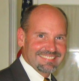
Mark W Haley
age ~69
from Albuquerque, NM
- Also known as:
-
- Mark I Haley
- Mark T Haley
- Mark C Haley
- Mark W Maley
- Terry Haley
- Mark Whaley
- Mark Y
- Phone and address:
-
7412 Don Tomas Ln NE, Albuquerque, NM 87109
(505)6606304
Mark Haley Phones & Addresses
- 7412 Don Tomas Ln NE, Albuquerque, NM 87109 • (505)6606304
- Rosanky, TX
- Eagle Nest, NM
- Rio Medina, TX
Work
-
Company:Johnson oil company inc2010
-
Position:Corporate credit and collection manager
Education
-
School / High School:Southwest Texas State University1987
-
Specialities:B.B.A.
Ranks
-
Licence:Texas - Eligible To Practice In Texas
-
Date:1983
Lawyers & Attorneys

Mark Rowland Haley - Lawyer
view sourceAddress:
(214)9699836 (Office)
Licenses:
Texas - Eligible To Practice In Texas 1983
Education:
Baylor University School of Law
Degree - Doctor of Jurisprudence/Juris Doctor (J.D.)
Graduated - 1982
Degree - Doctor of Jurisprudence/Juris Doctor (J.D.)
Graduated - 1982
Us Patents
-
Method For Cleaning Integrated Circuit Bonding Pads
view source -
US Patent:6355576, Mar 12, 2002
-
Filed:Apr 26, 1999
-
Appl. No.:09/299682
-
Inventors:Mark Haley - Rio Medina TX
Delbert Parks - Bexar TX
Judy Galloway - Fair Oaks TX -
Assignee:VLSI Technology Inc. - San Jose CA
-
International Classification:H01L 21461
-
US Classification:438745, 438725, 438704, 438974, 438963
-
Abstract:A method for cleaning bonding pads on a semiconductor device, as disclosed herein, includes treating the bonding pads with a CF and water vapor combination. In the process, the water vapor breaks up and the hydrogen from the water vapor couples to fluorine residue on the bonding pad surface creating a volatile HF vapor. In addition, fluorine from the CF exchanges with the titanium in the metallic polymer residue making the polymer more soluble for the organic strip operation which follows. Next, the resist is ashed and then an organic resist stripper is applied to the bonding pad area, thereby creating a clean bonding pad surface. Thereafter, a reliable bond wire connection can be made to the bonding pad.
-
Use Of Silicide Blocking Layer To Create High Valued Resistor And Diode For Sub-1V Bandgap
view source -
US Patent:6690083, Feb 10, 2004
-
Filed:Jun 1, 2000
-
Appl. No.:09/586411
-
Inventors:Todd Mitchell - San Antonio TX
Mark W. Haley - Rio Medina TX -
Assignee:Koninklijke Philips Electronics N.V. - Eindhoven
-
International Classification:H01L 2900
-
US Classification:257538, 257536, 257537, 257516, 257518
-
Abstract:The present invention is drawn to a method and a system for creating a sub-1V bandgap reference (BGR) circuit. In particular, a sub-1V BGR circuit is formed comprising a shallow trench isolation (STI) region and a poly silicon region above said STI region. The poly silicon region is formed having a first doped region longer than a second doped region. The poly silicon region as one single structure is adapted to function as a resistor and a diode coupled in series, said structure adapted to generate currents in a feedback loop to generate a BGR voltage. In forming the sub-1V BGR circuit, a silicide blocking mask (already available in the process flow for forming a standard semiconductor device) is used to prevent spacer oxide from forming above the center portion of the poly silicon region. In turn, silicide contacts can be formed away from the center portion of the poly silicon region.
-
Method And Apparatus For Cleaning Integrated Circuit Bonding Pads
view source -
US Patent:20020028586, Mar 7, 2002
-
Filed:Sep 21, 2001
-
Appl. No.:09/962045
-
Inventors:Mark Haley - Rio Medina TX, US
Delbert Parks - Bexar TX, US
Judy Galloway - Fair Oaks TX, US -
International Classification:H01L021/302
-
US Classification:438/784000, 438/734000, 438/780000, 438/782000
-
Abstract:A method for cleaning bonding pads on a semiconductor device, as disclosed herein, includes treating the bonding pads with a CFand water vapor combination. In the process, the water vapor breaks up and the hydrogen from the water vapor couples to fluorine residue on the bonding pad surface creating a volatile HF vapor. In addition, fluorine from the CFexchanges with the titanium in the metallic polymer residue making the polymer more soluble for the organic strip operation which follows. Next, the resist is ashed and then an organic resist stripper is applied to the bonding pad area, thereby creating a clean bonding pad surface. Thereafter, a reliable bond wire connection can be made to the bonding pad.
-
Technique And Apparatus For Testing Electrostatic Chucks
view source -
US Patent:59173270, Jun 29, 1999
-
Filed:Sep 8, 1997
-
Appl. No.:8/929172
-
Inventors:Mark W. Haley - Medina TX
Delbert H. Parks - San Antonio TX -
Assignee:VLSI Technology, Inc. - San Jose CA
-
International Classification:G01R 2912
H02N 1300 -
US Classification:324457
-
Abstract:A testing apparatus including a testing plate can be used to test an electrostatic wafer chuck. A DC potential is supplied so as to produce an electrostatic force. A mechanical force is supplied to the testing plate in order to give an indication of the produced electrostatic force. By examining the DC potential and the produced electrostatic force, an electrostatic wafer chuck can be qualified or rejected before being placed into a wafer processing machine. This reduces the possibility of damage to the wafer or the wafer processing machine.
-
Backend Process For Fuse Link Opening
view source -
US Patent:63067463, Oct 23, 2001
-
Filed:Dec 30, 1999
-
Appl. No.:9/475698
-
Inventors:Mark W. Haley - Rio Medina TX
Todd Mitchell - San Antonio TX -
Assignee:Koninklijke Philips Electronics - Eindhoven
-
International Classification:H01L 2144
-
US Classification:438601
-
Abstract:The present invention is directed to a method of forming an insulative layer over a fuse link in a semiconductor device that is sufficiently thick to encapsulate the fuse link during laser opening, thereby preventing vaporized metal from re-depositing on the fuse link. The layer is also sufficiently thin to allow the laser to penetrate the insulative layer during laser opening of the fuse. A primary dielectric layer is formed over a metal fuse link, the primary dielectric having a predetermined deposition thickness over the fuse link. The primary dielectric layer is then covered with an etch interrupting layer. The etch interrupting layer is covered with a secondary dielectric layer and a portion of the secondary dielectric layer is then removed, resulting in an interlayer dielectric (ILD) stack formed from the etch interrupting layer and the remaining secondary dielectric layer. The ILD has a selected thickness that is greater than the thickness of the primary dielectric layer. A metal layer is formed over the interlayer dielectric and then the layers over the etch interrupting layer and above the metal fuse link are then removed.
-
Multiple Pole Electrostatic Chuck With Self Healing Mechanism For Wafer Clamping
view source -
US Patent:59532009, Sep 14, 1999
-
Filed:Feb 5, 1998
-
Appl. No.:9/019458
-
Inventors:Mark W. Haley - Rio Medina TX
Albert H. Liu - San Antonio TX -
Assignee:VLSI Technology, Inc. - San Jose CA
-
International Classification:H02N 1300
-
US Classification:361234
-
Abstract:An electrostatic chuck device for clamping a semiconductor wafer substrate during processing of the semiconductor wafer includes a power source, at least one negative pole, and a plurality of positive poles. Each positive pole selected from the plurality of positive poles is electrically separated from the negative pole. Also provided is a plurality of fuses, each fuse of the plurality of fuses is coupled to an associated positive pole included in the plurality of positive poles. Each fuse is further coupled to the power source. In some embodiments, each positive pole is electrically separated from the negative pole by an insulating epoxy. In other embodiments, the plurality of positive poles are connected to each other in parallel.
-
Converter And Digital Channel Selector
view source -
US Patent:56002360, Feb 4, 1997
-
Filed:Nov 1, 1994
-
Appl. No.:8/333009
-
Inventors:Mark W. Haley - San Antonio TX
Eric A. Sparks - San Antonio TX -
Assignee:VLAI Technology, Inc. - San Jose CA
-
International Classification:G01R 104
-
US Classification:3241581
-
Abstract:A converter and digital channel selector device is provided which is interconnected between a source measurement unit having a plurality of output terminal connectors and a probe station having a plurality of input probe terminal connectors. The channel selector device is used to selectively connect each one of the plurality of output terminals of the source measurement unit to corresponding one of the plurality of input probe terminal connectors, respectively. The channel selector device includes a converter for generating a plurality of digital control signals and a digital channel select logic circuit which is responsive to the digital control signals for selectively connecting respective ones of a plurality of its input channel connectors connected to the plurality of output terminal connectors to any one of a plurality of its output channel connectors connected to the plurality of input probe terminal connectors.
Name / Title
Company / Classification
Phones & Addresses
Owner
Mark Haley Roofing
Roofing Contractors
Roofing Contractors
2001 Ferndale Road, Victoria, BC V8N 2Y4
(250)7215345
(250)7215345
Owner
Mark Haley Roofing
Roofing Contractors
Roofing Contractors
(250)7215345
Vice President
KIWANIS CLUB OF ALBUQUERQUE, NEW MEXICO, INC
PO Box 21517, Albuquerque, NM 87154
4333 Pan American Fwy , Albuquerque, NM 87107
4333 Pan American Fwy , Albuquerque, NM 87107
Haley & Son Hot Tub Movers
Hauling Services · Moving Companies · Pool Cleaners
Hauling Services · Moving Companies · Pool Cleaners
1840 Southern Blvd SE, Rio Rancho, NM 87124
3225 21 Ave SE, Rio Rancho, NM 87124
(505)8910117
3225 21 Ave SE, Rio Rancho, NM 87124
(505)8910117
Vice-President
Cauwels & Stuve Realty & Development Advisors
Real Estate Agent/Manager · Nonresidential Building Operators
Real Estate Agent/Manager · Nonresidential Building Operators
6001 Indian School Rd NE, Albuquerque, NM 87110
8814 Horizon Blvd NE, Albuquerque, NM 87113
(505)2665711
8814 Horizon Blvd NE, Albuquerque, NM 87113
(505)2665711
President
SPEED OF LIGHT SALES, INC
PO Box 27189, Albuquerque, NM 87125
3300 Princeton NE, Albuquerque, NM 87107
3300 Princeton NE, Albuquerque, NM 87107
President
LIGHTING SERVICES, INC
PO Box 27189, Albuquerque, NM 87125
6200 Uptown Blvd Ne , Albuquerque, NM 87110
6200 Uptown Blvd Ne , Albuquerque, NM 87110
Secretary
TRANSWEST SERVICES, INC
PO Box 27189, Albuquerque, NM 87102
3300 Princeton Ne , Albuquerque, NM 87110
3300 Princeton Ne , Albuquerque, NM 87110
Medicine Doctors

Mark M. Haley
view sourceSpecialties:
Family Medicine
Work:
Campus Health & Well-Being
1 Grand Ave BLDG 27, San Luis Obispo, CA 93410
(805)7561211 (phone), (805)7565298 (fax)
1 Grand Ave BLDG 27, San Luis Obispo, CA 93410
(805)7561211 (phone), (805)7565298 (fax)
Languages:
Chinese
English
Spanish
English
Spanish
Description:
Mr. Haley works in San Luis Obispo, CA and specializes in Family Medicine.
Resumes

Mark Haley San Marcos, TX
view sourceWork:
Johnson Oil Company Inc
2010 to 2000
Corporate Credit and Collection Manager Cash Box Motors LLC. & Advanced Production Solutions
2008 to 2010
Business Operations Consultant Xanadoo Wireless Services
Wichita Falls, TX
2005 to 2008
Director and Regional General Manager Grande Communications Inc
Austin, TX
2002 to 2005
Sr. Manager of Business Operations RLX Technologies Inc
The Woodlands, TX
2001 to 2002
Corporate Customer Service Manager Vignette Corporation
Austin, TX
2000 to 2001
Corporate Credit and Collection Manager Texas Instruments Inc. - Texas Division
Austin, TX
1994 to 2000
Credit and Collection Manager Commercial Metals Company, Steel Group
Seguin, TX
1990 to 1994
Assistant Corporate Credit Manager Tex Marketing
Austin, TX
1989 to 1990
Customer Service Supervisor Ford Motor Credit
San Antonio, TX
1988 to 1989
Customer Service Representative
Education:
Southwest Texas State University
1987
B.B.A.
1987
B.B.A.
Googleplus

Mark Haley
Work:
Federal Reserve Board - Senior Financial Services Analyst
Education:
Brandeis International Business School - International Economics and Finance, Grinnell College - Economics, Paul H. Nitze School of Advanced International Studies - International Studies

Mark Haley
Work:
Pro Cut Llc - Taking over Vegas 1 job at a time
About:
Work hard play hard no time for looser's

Mark Haley
About:
We are a full service Security consulting firm. We offer Executive protection and the training of Dual Purpose Police Canines for the Law Enforcement Community as well as the private sector.
Tagline:
Law Enforcement and Security certified Instructor

Mark Haley
Tagline:
Running Puppies-UK website for 15 Years

Mark Haley

Mark Haley

Mark Haley

Mark Haley
Myspace

Johnathan Mark Haley
view sourceFriends:
Theresa Clancy Scholes, Bob Haley, Joshua Haley, Christine Blackburn

Mark Haley Providence RI
view sourceMark Haley (Providence, RI)

Mark Haley Portland OR
view sourceFriends:
Christopher Healy, Jamie VanDrunen, Angie Pino McKeague
Mark Haley (Portland, OR)

Mark Haley
view source
Mark Haley Wilmingt DE
view sourceFriends:
Ed Dwornik, Scott Hudson, Tina Michini, Gabe Haley, Jason Hill
Mark Haley (Wilmington, DE)

Mark Haley Leeds
view sourceFriends:
Jason Pennock, Ryan Tiffany, Andy Heward, Jenny Rogers-Thomas
Mark Haley (Leeds)

Mark Haley Austria
view sourceMark Haley (Austria)

Mark Haley Ld
view sourceFriends:
Jules Haley, Matthew Burchell, Ian Honnor, Fred 'Fly' Hunt
Mark Haley (London)
Classmates

Mark Haley
view sourceSchools:
Ridgeview High School Atlanta GA 1976-1980
Community:
Allison Henning, Heidi Morton, Jolie Ellis, Bill Owen

Mark Haley
view sourceSchools:
Bishop Ireton High School Alexandria VA 1980-1984
Community:
Jeff Mcgrath, Christine Wells, Fred Hopewell, Denise Jardin, John Trippel

Mark Haley
view sourceSchools:
Ridgeview High School Atlanta GA 1976-1980
Community:
Allison Henning, Heidi Morton, Jolie Ellis, Bill Owen

Mark Haley
view sourceSchools:
Waco High School Waco TX 1997-2001
Community:
Marlys Stewart, Gary Dowdall

Mark Haley
view sourceSchools:
Peterborough Elementary School Peterborough NH 1990-1994, Peterborough Middle School Peterborough NH 1994-1998
Community:
Amy Laber, Jerry Ambroze

Mark Haley
view sourceSchools:
Roberto Clemente Intermediate School 195 New York NY 1991-1993

Mark Haley
view sourceSchools:
Jackman Middle School Newburyport MA 1971-1971
Community:
Cheryl Koncal, Mike Dziekonski, Joyce Lapan, Karen Ball

Mark Haley
view sourceSchools:
Chenango Valley Central High School Binghamton NY 1974-1978
Community:
Kathy Clarke, Mary Webb, Donna Throup, Cindy Smey
Youtube
Flickr
Plaxo

Mark Haley
view sourceHamiltonAVP - Human Resources Services at McMaster Univers... Past: Vice-President – Human Resources Management Services at Provincial Health Authorities of... Seasoned Human Resources executive in a large and complex organization which employs 13,000 people.

Mark Haley
view sourceTacoma Washington USAManaging Director, International at Snack Alliance... Past: Interim Exec Director at Bellevue Arts Museum, Chairman & CEO at Brown Haley, President &...

Mark Haley
view sourceAtlanta, GA

Mark Haley
view sourceDorchester, MA

Mark Haley
view source
Mark D. Haley
view sourceAtlanta., GA

Mark Haley
view sourceBoston, MA

Mark Winston Haley
view sourceCauwels Stuve Relaty and Development Advisors L L...
Get Report for Mark W Haley from Albuquerque, NM, age ~69


![But That_s Another Day] Karley Kemp Mark Rangel Se... But That_s Another Day] Karley Kemp Mark Rangel Se...](https://i.ytimg.com/vi/PrAtG_ubt2c/hq720.jpg?sqp=-oaymwE2CNAFEJQDSFXyq4qpAygIARUAAIhCGAFwAcABBvABAfgB_gmAAtAFigIMCAAQARhyIGMoOTAP&rs=AOn4CLBD5iWKNKdhcSzzlmVuq4OsRRCyKA)


