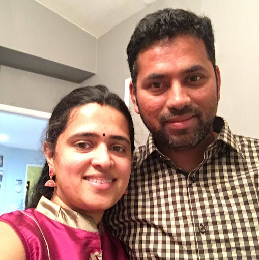
Ramkumar K Subramanian
age ~47
from Fremont, CA
- Also known as:
-
- Ramkumar K Subramaniam
- Ram Kumar Subramanian
- Kumar Subramanian Ramkumar
- Ramkumar Subramnian
- Ram K Subramanian
- Ramirez K Subramanian
- Kumar Subramanian Ramirez
- Subramanian Pod Ramkumar
- Subramanian Ramkumar
Ramkumar Subramanian Phones & Addresses
- Fremont, CA
- Union City, CA
- Lafayette, CO
- Euless, TX
- Revere, MA
- Dallas, TX
- Arlington, TX
- Pittsburgh, PA
- Miami, FL
- Cookeville, TN
Work
-
Company:Corporate strategy, amdJan 2010
-
Position:Director and high growth market strategist
Education
-
School / High School:Duke University- Durham, NC2002
-
Specialities:MBA in General Management, Finance & Marketing
Resumes

Srsme At At&T
view sourcePosition:
SrSME at AT&T
Location:
San Francisco Bay Area
Industry:
Information Technology and Services
Work:
AT&T
SrSME
SrSME

Ramkumar Subramanian
view sourceLocation:
Schaumburg, Illinois
Industry:
Information Technology and Services

Ramkumar Subramanian Austin, TX
view sourceWork:
Corporate Strategy, AMD
Jan 2010 to 2000
Director and High Growth Market Strategist AMD India Pvt. Ltd
Bangalore, Karnataka
Sep 2008 to Dec 2009
Regional Vice-President, Sales & Marketing; Director High Growth Markets
Sunnyvale, CA
Sep 2003 to Sep 2008
Manager, Sr. Manager, Director, Corporate Development Development Center, AMD
Sunnyvale, CA
Dec 1995 to Sep 2003
Sr. Engineer, MTS, Sr. MTS, Manufacturing and Process Development Procter & Gamble
Cincinnati, OH
Mar 1992 to Jun 1992
Process Engineer
Education:
Duke University
Durham, NC
2002
MBA in General Management, Finance & Marketing Michigan State University
East Lansing, MI
1995
PhD in Chemical Engineering Michigan State University
East Lansing, MI
1992
MS in Chemical Engineering National Institute of Technology
1989
B. Tech in Chemical Technology
Durham, NC
2002
MBA in General Management, Finance & Marketing Michigan State University
East Lansing, MI
1995
PhD in Chemical Engineering Michigan State University
East Lansing, MI
1992
MS in Chemical Engineering National Institute of Technology
1989
B. Tech in Chemical Technology
Us Patents
-
Use Of Rta Furnace For Photoresist Baking
view source -
US Patent:6335152, Jan 1, 2002
-
Filed:May 1, 2000
-
Appl. No.:09/564408
-
Inventors:Ramkumar Subramanian - San Jose CA
Bharath Rangarajan - Santa Clara CA
Michael K. Templeton - Atherton CA
Bhanwar Singh - Morgan Hill CA -
Assignee:Advanced Micro Devices, Inc. - Sunnyvale CA
-
International Classification:G03F 738
-
US Classification:430325, 430328, 430330
-
Abstract:In one embodiment, the present invention relates to a method of processing an irradiated photoresist involving the steps of placing a substrate having the irradiated photoresist thereon at a first temperature in a rapid thermal anneal furnace; heating the substrate having the irradiated photoresist thereon to a second temperature within about 0. 1 seconds to about 10 seconds; cooling the substrate having the irradiated photoresist thereon to a third temperature in a rapid thermal annealing furnace within about 0. 1 seconds to about 10 seconds; and developing the irradiated photoresist, wherein the second temperature is higher than the first temperature and the third temperature. In another embodiment, the present invention relates to a system of processing a photoresist, containing a source of actinic radiation and a mask for selectively irradiating a photoresist; a rapid thermal annealing furnace for rapidly heating and rapidly cooling a selectively irradiated photoresist, wherein the rapid heating and rapid cooling are independently conducted within about 0. 1 seconds to about 10 seconds; and a developer for developing a rapid thermal annealing furnace heated and selectively irradiated photoresist into a patterned photoresist.
-
Method Of Forming Self-Aligned Contacts Using Consumable Spacers
view source -
US Patent:6348379, Feb 19, 2002
-
Filed:Feb 11, 2000
-
Appl. No.:09/502153
-
Inventors:Fei Wang - San Jose CA
Ramkumar Subramanian - San Jose CA
Yu Sun - Saratoga CA -
Assignee:Advanced Micro Devices, Inc. - Sunnyvale CA
-
International Classification:H01L 21336
-
US Classification:438257, 438263, 438264, 438265
-
Abstract:A method for shrinking a semiconductor device is disclosed. An etch stop layer is eliminated and is replaced with a consumable second sidewall spacers so that stacked gate structures of the device can be positioned closer together, thus permitting shrinking of the device. In a preferred embodiment, the present invention provides a method for forming self-aligned contacts by forming multi-layer structures on a region on a semiconductor substrate, forming first sidewall spacers around the multi-layer structures, forming second sidewall spacers around the first sidewall spacers, forming a dielectric layer directly over the substrate and in contact with second sidewall spacers, forming an opening in the dielectric layer to expose a portion of the region on the semiconductor substrate adjacent the second sidewall spacers, and filling the opening with a conductive material to form a contact.
-
Method For Using A Low Dielectric Constant Layer As A Semiconductor Anti-Reflective Coating
view source -
US Patent:6348406, Feb 19, 2002
-
Filed:May 31, 2000
-
Appl. No.:09/586264
-
Inventors:Ramkumar Subramanian - San Jose CA
Minh Van Ngo - Fremont CA
Kashmir Sahota - Fremont CA
Yongzhong Hu - San Jose CA
Hiroyuki Kinoshita - Sunnyvale CA
Fei Wang - San Jose CA
Wenge Yang - Fremont CA -
Assignee:Advanced Micro Devices, Inc. - Sunnyvale CA
-
International Classification:H01L 214763
-
US Classification:438636, 438631, 438633, 438637
-
Abstract:The present invention provides a method for manufacturing a semiconductor device with an anti-reflective coating (ARC) that does not need to be removed. In one embodiment, electrical devices are formed on a semiconductor substrate. A dielectric layer is then deposited over the electrical devices and the semiconductor substrate, upon which an optically transparent ARC layer of low dielectric constant is then deposited. Photoresist is then deposited on top of the ARC layer and is then photolithographically processed and subsequently developed. The dielectric layer is then etched down to the semiconductor substrate to form contacts or local interconnects. The ARC layer can subsequently be used as a hard mask and does not require removal.
-
Use Of Carbon Nanotubes To Calibrate Conventional Tips Used In Afm
view source -
US Patent:6354133, Mar 12, 2002
-
Filed:Dec 4, 2000
-
Appl. No.:09/729293
-
Inventors:Sanjay K. Yedur - San Ramon CA
Bhanwar Singh - Morgan Hill CA
Bryan K. Choo - Mountain View CA
Michael K. Templeton - Atherton CA
Ramkumar Subramanian - Sunnyvale CA -
Assignee:Advanced Micro Devices, Inc. - Sunnyvale CA
-
International Classification:G01B 528
-
US Classification:73 189
-
Abstract:The present invention provides systems, methods, and standards for calibrating nano-measuring devices. Calibration standards of the invention include carbon nanotubes and methods of the invention involve scanning carbon nanotubes using nano-scale measuring devices. The widths of the carbon nanotube calibration standards are known with a high degree of accuracy. The invention allows calibration of a wide variety of nano-scale measuring devices, taking into account many, and in some cases all, of the systematic errors that may affect a nano-scale measurement. The invention may be used to accurately calibrate line width, line height, and trench width measurements and may be used to precisely characterize both scanning probe microscope tips and electron microscope beams.
-
Bright Field Image Reversal For Contact Hole Patterning
view source -
US Patent:6358856, Mar 19, 2002
-
Filed:Nov 21, 2000
-
Appl. No.:09/716215
-
Inventors:Christopher F. Lyons - Fremont CA
Ramkumar Subramanian - Sunnyvale CA
Marina V. Plat - San Jose CA
Todd P. Lukanc - San Jose CA -
Assignee:Advanced Micro Devices, Inc. - Sunnyvale CA
-
International Classification:H01L 21311
-
US Classification:438703, 438713
-
Abstract:A method of forming a small contact hole uses a bright field mask to form a small cylinder in a positive resist layer. A negative resist layer is formed around the small cylinder, and then etched or polished back to leave a top portion of the small cylinder exposed above the negative resist layer. The negative resist layer and the small cylinder (positive resist) are flood exposed to light, and then subject to a developer. What remains is a small contact hole located where the small cylinder was previously located.
-
Method Of Making A Slot Via Filled Dual Damascene Structure With Middle Stop Layer
view source -
US Patent:6365505, Apr 2, 2002
-
Filed:Feb 21, 2001
-
Appl. No.:09/780531
-
Inventors:Fei Wang - San Jose CA
Lynne A. Okada - Sunnyvale CA
Ramkumar Subramanian - San Jose CA
Calvin T. Gabriel - Cupertino CA -
Assignee:Advanced Micro Devices, Inc. - Sunnyvale CA
-
International Classification:H01L 214763
-
US Classification:438624, 438634, 438637, 438638, 438666, 438668, 438672, 438687
-
Abstract:A method of forming an interconnect structure in which an inorganic low k dielectric material is deposited over a conductive layer to form a first dielectric layer. An etch stop layer is formed on the first dielectric layer. The etch stop layer and the first dielectric layer are etched to form a slot via in the first dielectric layer. The slot via is longer than the width of a subsequently formed trench. An organic low k dielectric material is deposited within the slot via and over the etch stop layer to form a second dielectric layer over the slot via and the etch stop layer. The re-filled slot via is simultaneously etched with the second dielectric layer in which a trench is formed. The entire width of the trench is directly over the via. The re-opened via and the trench are filled with a conductive material.
-
Semiconductor Manufacturing Method Using A Dielectric Photomask
view source -
US Patent:6365509, Apr 2, 2002
-
Filed:May 31, 2000
-
Appl. No.:09/586556
-
Inventors:Ramkumar Subramanian - San Jose CA
Wenge Yang - Fremont CA
Marina V. Plat - San Jose CA
Lewis Shen - Cupertino CA -
Assignee:Advanced Micro Devices, Inc. - Sunnyvale CA
-
International Classification:H01L 214763
-
US Classification:438636, 438703, 438734, 438737, 438738, 438637, 438624
-
Abstract:A method is provided for manufacturing a semiconductor with fewer steps and minimized variation in the etching process by using SiON as a bottom antireflective (BARC) layer and hard mask in conjunction with a thin photoresist layer. In one embodiment, an etch-stop layer is deposited on a semiconductor substrate, a dielectric layer is deposited on top of the etch-stop layer, a BARC is deposited on top of the dielectric layer, and a photoresist layer with a thickness less than the thickness of the BARC is then deposited on top of the BARC. The photoresist is then patterned, photolithographically processed, and developed. The BARC is then etched away in the pattern developed on the photoresist and to photoresist is then removed. The BARC is then used as a mask for the etching of the dielectric layer and is subsequently removed in the process of etchings the dielectric and etch-stop layers without the benefit of a separate BARC-removal step.
-
Ozone Cleaning Of Wafers
view source -
US Patent:6371134, Apr 16, 2002
-
Filed:Jan 31, 2000
-
Appl. No.:09/495014
-
Inventors:Ramkumar Subramanian - San Jose CA
Khoi A. Phan - San Jose CA
Bharath Rangarajan - Santa Clara CA
Bhanwar Singh - Morgan Hill CA
Sanjay K. Yedur - Santa Clara CA
Bryan K. Choo - Mountain View CA -
Assignee:Advanced Micro Devices, Inc. - Sunnyvale CA
-
International Classification:B08B 700
-
US Classification:134 12, 134 11, 134 13, 134 26, 134 29
-
Abstract:In one embodiment, the present invention relates to a method of processing a semiconductor structure, involving the steps of providing the semiconductor structure having a patterned resist thereon; stripping the patterned resist from the semiconductor structure, wherein an amount of carbon containing resist debris remain on the semiconductor structure; and contacting the semiconductor structure with ozone thereby reducing the amount of carbon containing resist debris thereon.
Classmates

Ramkumar Subramanian | Ea...
view source
Ramkumar Subramanian
view source
Ramkumar Subramanian
view source
Ramkumar Subramanian
view source
Ramkumar Subramanian
view source
Ramkumar Subramanian
view source
Ramkumar Subramanian
view source
Ramkumar Subramanian
view source
Ramkumar Subramanian
view sourcePlaxo

Ramkumar Subramanian
view sourceCambridge, MA, USA

ramkumar subramanian
view source24/7 Customer
Youtube
Googleplus

Ramkumar Subramanian

Ramkumar Subramanian

Ramkumar Subramanian

Ramkumar Subramanian

Ramkumar Subramanian

Ramkumar Subramanian

Ramkumar Subramanian

Ramkumar Subramanian
Flickr
Get Report for Ramkumar K Subramanian from Fremont, CA, age ~47


