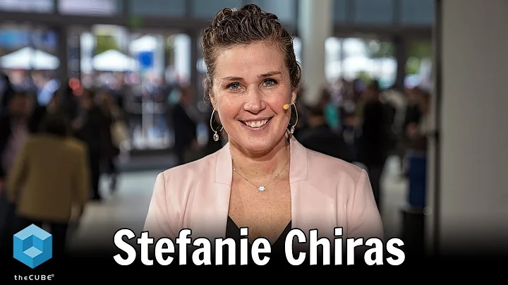
Stefanie Ruth Chiras
age ~54
from Groton, MA
- Also known as:
-
- Stefanie R Chiras
- Stephanie R Chiras
- Stef Chiras
- Chiras Stef
- Phone and address:
- 7 Overlook Dr, Groton, MA 01450
Stefanie Chiras Phones & Addresses
- 7 Overlook Dr, Groton, MA 01450
- 34 Providence St, Millbury, MA 01527 • (508)8654260 • (508)8654883
- 3917 Knob Creek Ln, Cedar Park, TX 78613 • (609)7161460
- 329 Smith St, Peekskill, NY 10566
- 1810 Baldwin Rd, Yorktown Heights, NY 10598
- 1870 Baldwin Rd #20, Yorktown Heights, NY 10598
- Plainsboro, NJ
- Goleta, CA
- Westchester, NY
- Acton, MA
- 3917 Knob Creek Ln, Cedar Park, TX 78613
Work
-
Position:Sales Occupations
Us Patents
-
Structure To Improve Adhesion Between Top Cvd Low-K Dielectric And Dielectric Capping Layer
view source -
US Patent:7102232, Sep 5, 2006
-
Filed:Apr 19, 2004
-
Appl. No.:10/827693
-
Inventors:Lawrence A. Clevenger - LaGrangeville NY, US
Stefanie R. Chiras - Peekskill NY, US
Timothy Dalton - Ridgefield CT, US
James J. Demarest - Fishkill NY, US
Derren N. Dunn - Fishkill NY, US
Chester T. Dziobkowski - Hopewell Junction NY, US
Philip L. Flaitz - Newburgh NY, US
Michael W. Lane - Cortlandt Manor NY, US
James R. Lloyd - Katonah NY, US
Darryl D. Restaino - Modena NY, US
Thomas M. Shaw - Peekskill NY, US
Yun-Yu Wang - Poughquag NY, US
Chih-Chao Yang - Beacon NY, US -
Assignee:International Business Machines Corporation - Armonk NY
-
International Classification:H01L 23/52
-
US Classification:257751, 257758, 257753, 257E2316, 257E21584
-
Abstract:An interconnect structure in which the adhesion between an upper level low-k dielectric material, such as a material comprising elements of Si, C, O, and H, and an underlying diffusion capping dielectric, such as a material comprising elements of C, Si, N and H, is improved by incorporating an adhesion transition layer between the two dielectric layers. The presence of the adhesion transition layer between the upper level low-k dielectric and the diffusion barrier capping dielectric can reduce the chance of delamination of the interconnect structure during the packaging process. The adhesion transition layer provided herein includes a lower SiO— or SiON-containing region and an upper C graded region. Methods of forming such a structure, in particularly the adhesion transition layer, are also provided.
-
Copper Conductor
view source -
US Patent:7119018, Oct 10, 2006
-
Filed:Jul 9, 2004
-
Appl. No.:10/887087
-
Inventors:Michael W. Lane - Cortlandt Manor NY, US
Stefanie R. Chiras - Peekskill NY, US
Terry A. Spooner - New Fairfield CT, US
Robert Rosenberg - Cortlandt Manor NY, US
Daniel C. Edelstein - White Plains NY, US -
Assignee:International Buisness Machines Corporation - Armonk NY
-
International Classification:H01L 21/44
-
US Classification:438686, 438687, 438E23005
-
Abstract:A conducting material comprising: a conducting core region comprising copper and from 0. 001 atomic percent to 0. 6 atomic percent of one or more metals selected from iridium, osmium and rhenium; and an interfacial region. The interfacial region comprises at least 80 atomic percent or greater of the one or more metals. The invention is also directed to a method of making a conducting material comprising: providing an underlayer; contacting the underlayer with a seed layer, the seed layer comprising copper and one or more metals selected from iridium, osmium and rhenium; depositing a conducting layer comprising copper on the seed layer, and annealing the conducting layer at a temperature sufficient to cause grain growth in the conducting layer, yet minimize the migration of the one or more alloy metals from the seed layer to the conducting layer. The method further comprises polishing the conducting layer to provide a polished copper surface material, and annealing the polished copper surface material at a temperature to cause migration of the one or more metals from the seed layer to the polished surface to provide an interfacial region in contact with a copper conductor core region. The interfacial region and the copper conductor core region comprise the one or more metals.
-
Electroplated Cowp Composite Structures As Copper Barrier Layers
view source -
US Patent:7193323, Mar 20, 2007
-
Filed:Nov 18, 2003
-
Appl. No.:10/714966
-
Inventors:Cyril Cabral, Jr. - Ossining NY, US
Stefanie R. Chiras - Peekskill NY, US
Emanuel Cooper - Scarsdale NY, US
Hariklia Deligianni - Tenafly NY, US
Andrew J. Kellock - Sunnyvale CA, US
Judith M. Rubino - Ossining NY, US
Roger Y. Tsai - Yorkstown Heights NY, US -
Assignee:International Business Machines Corporation - Armonk NY
-
International Classification:H01L 23/48
H01L 23/52 -
US Classification:257751, 257752, 257762
-
Abstract:A composite material comprising a layer containing copper, and an electrodeposited CoWP film on the copper layer. The CoWP film contains from 11 atom percent to 25 atom percent phosphorus and has a thickness from 5 nm to 200 nm. The invention is also directed to a method of making an interconnect structure comprising: providing a trench or via within a dielectric material, and a conducting metal containing copper within the trench or the via; and forming a CoWP film by electrodeposition on the copper layer. The CoWP film contains from 10 atom percent to 25 atom percent phosphorus and has a thickness from 5 nm to 200 nm. The invention is also directed to a interconnect structure comprising a dielectric layer in contact with a metal layer; an electrodeposited CoWP film on the metal layer, and a copper layer on the CoWP film.
-
Electroplated Cowp Composite Structures As Copper Barrier Layers
view source -
US Patent:7217655, May 15, 2007
-
Filed:Feb 2, 2005
-
Appl. No.:11/047652
-
Inventors:Cyril Cabral, Jr. - Mahopac NY, US
Stefanie R. Chiras - Peekskill NY, US
Emanuel I. Cooper - Scarsdale NY, US
Hariklia Deligianni - Tenafly NJ, US
Andrew J. Kellock - Sunnyvale CA, US
Judith M. Rubino - Ossining NY, US
Roger Y. Tsai - Yorktown Heights NY, US -
Assignee:International Business Machines Corporation - Armonk NY
-
International Classification:H01L 21/4763
-
US Classification:438642, 438637, 438648, 438675, 438687, 257E21585
-
Abstract:A composite material comprising a layer containing copper, and an electrodeposited CoWP film on the copper layer. The CoWP film contains from 11 atom percent to 25 atom percent phosphorus and has a thickness from 5 nm to 200 nm. The invention is also directed to a method of making an interconnect structure comprising: providing a trench or via within a dielectric material, and a conducting metal containing copper within the trench or the via; and forming a CoWP film by electrodeposition on the copper layer. The CoWP film contains from 10 atom percent to 25 atom percent phosphorus and has a thickness from 5 nm to 200 nm. The invention is also directed to a interconnect structure comprising a dielectric layer in contact with a metal layer; an electrodeposited CoWP film on the metal layer, and a copper layer on the CoWP film.
-
Ball Limiting Metallurgy, Interconnection Structure Including The Same, And Method Of Forming An Interconnection Structure
view source -
US Patent:7273803, Sep 25, 2007
-
Filed:Dec 1, 2003
-
Appl. No.:10/724938
-
Inventors:Yu-Ting Cheng - HsinChu, TW
Stefanie Ruth Chiras - Peekskill NY, US
Donald W. Henderson - Ithaca NY, US
Sung-Kwon Kang - Chappaqua NY, US
Stephen James Kilpatrick - Olney MD, US
Carlos J. Sambucetti - Vallejo CA, US
Da-Yuan Shih - Poughkeepsie NY, US -
Assignee:International Business Machines Corporation - Armonk NY
-
International Classification:H01L 21/44
-
US Classification:438612
-
Abstract:A ball-limiting metallurgy includes a substrate, a barrier layer formed over the substrate, an adhesion layer formed over the barrier layer, a first solderable layer formed over the adhesion layer, a diffusion barrier layer formed over the adhesion layer, and a second solderable layer formed over the diffusion barrier layer.
-
Structure To Improve Adhesion Between Top Cvd Low-K Dielectric And Dielectric Capping Layer
view source -
US Patent:7402532, Jul 22, 2008
-
Filed:Aug 4, 2006
-
Appl. No.:11/499220
-
Inventors:Lawrence A. Clevenger - LaGrangeville NY, US
Stefanie R. Chiras - Peekskill NY, US
Timothy Dalton - Ridgefield CT, US
James J. Demarest - Fishkill NY, US
Derren N. Dunn - Fishkill NY, US
Chester T. Dziobkowski - Hopewell Junction NY, US
Philip L. Flaitz - Newburgh NY, US
Michael W. Lane - Cortlandt Manor NY, US
James R. Lloyd - Katonah NY, US
Darryl D. Restaino - Modena NY, US
Thomas M. Shaw - Peekskill NY, US
Yun-Yu Wang - Poughquag NY, US
Chih-Chao Yang - Beacon NY, US -
Assignee:International Business Machines Corporation - Armonk NY
-
International Classification:H01L 23/48
-
US Classification:438783, 257E21576
-
Abstract:An interconnect structure in which the adhesion between an upper level low-k dielectric material, such as a material comprising elements of Si, C, O, and H, and an underlying diffusion capping dielectric, such as a material comprising elements of C, Si, N and H, is improved by incorporating an adhesion transition layer between the two dielectric layers. The presence of the adhesion transition layer between the upper level low-k dielectric and the diffusion barrier capping dielectric can reduce the chance of delamination of the interconnect structure during the packaging process. The adhesion transition layer provided herein includes a lower SiO- or SiON-containing region and an upper C graded region. Methods of forming such a structure, in particularly the adhesion transition layer, are also provided.
-
Metal Capped Copper Interconnect
view source -
US Patent:7495338, Feb 24, 2009
-
Filed:Mar 16, 2006
-
Appl. No.:11/376199
-
Inventors:Michael Lane - Cortlandt Manor NY, US
Stefanie R. Chiras - Peekskill NY, US
Terry A. Spooner - New Fairfield CT, US
Robert Rosenberg - Cortlandt Manor NY, US
Daniel C. Edelstein - White Plains NY, US -
Assignee:International Business Machines Corporation - Armonk NY
-
International Classification:H01L 29/40
-
US Classification:257762, 257767
-
Abstract:A conducting material comprising: a conducting core region comprising copper and from 0. 001 atomic percent to 0. 6 atomic percent of one or more metals selected from iridium, osmium and rhenium; and an interfacial region. The interfacial region comprises at least 80 atomic percent or greater of the one or more metals. The invention is also directed to a method of making a conducting material comprising: providing an underlayer; contacting the underlayer with a seed layer, the seed layer comprising copper and one or more metals selected from iridium, osmium and rhenium; depositing a conducting layer comprising copper on the seed layer, and annealing the conducting layer at a temperature sufficient to cause grain growth in the conducting layer, yet minimize the migration of the one or more alloy metals from the seed layer to the conducting layer. The method further comprises polishing the conducting layer to provide a polished copper surface material, and annealing the polished copper surface material at a temperature to cause migration of the one or more metals from the seed layer to the polished surface to provide an interfacial region in contact with a copper conductor core region. The interfacial region and the copper conductor core region comprise the one or more metals.
-
Structure To Improve Adhesion Between Top Cvd Low-K Dielectric And Dielectric Capping Layer
view source -
US Patent:7820559, Oct 26, 2010
-
Filed:Jun 23, 2008
-
Appl. No.:12/143917
-
Inventors:Lawrence A. Clevenger - LaGrangeville NY, US
Stefanie R. Chiras - Peekskill NY, US
Timothy Dalton - Ridgefield CT, US
James J. Demarest - Fishkill NY, US
Darren N. Dunn - Fishkill NY, US
Chester T. Dziobkowski - Hopewell Junction NY, US
Philip L. Flaitz - Newburgh NY, US
Michael W. Lane - Cortlandt Manor NY, US
James R. Lloyd - Katonah NY, US
Darryl D. Restaino - Modena NY, US
Thomas M. Shaw - Peekskill NY, US
Yun-Yu Wang - Poughquag NY, US
Chih-Chao Yang - Beacon NY, US -
Assignee:International Business Machines Corporation - Armonk NY
-
International Classification:H01L 21/31
H01L 21/4763 -
US Classification:438783, 438654, 257E21576
-
Abstract:An interconnect structure in which the adhesion between an upper level low-k dielectric material, such as a material comprising elements of Si, C, O, and H, and an underlying diffusion capping dielectric, such as a material comprising elements of C, Si, N and H, is improved by incorporating an adhesion transition layer between the two dielectric layers. The presence of the adhesion transition layer between the upper level low-k dielectric and the diffusion barrier capping dielectric can reduce the chance of delamination of the interconnect structure during the packaging process. The adhesion transition layer provided herein includes a lower SiO— or SiON-containing region and an upper C graded region. Methods of forming such a structure, in particularly the adhesion transition layer, are also provided.
News

IBM unveils Power8 Linux servers for deep learning
view source- The new systems tap the Nvidia NVLink technology to move data five times faster than any competing platform, said Stefanie Chiras, an IBM vice president, in an interview with VentureBeat. These systems and their operating systems are part of a larger business group that generates about $2 billion a
- Date: Sep 08, 2016
- Category: Sci/Tech
- Source: Google
Youtube
Get Report for Stefanie Ruth Chiras from Groton, MA, age ~54


