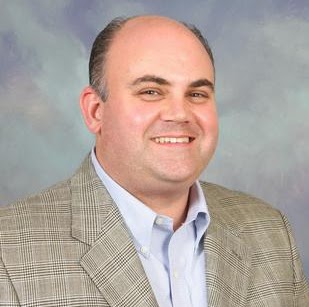
Stephen H Krause
age ~72
from Jaffrey, NH
- Also known as:
-
- Stephen Holden Krause
- Stephen Krause Ret
- Steve H Krause
- Stephen Krauss
- Marie O'Brien
Stephen Krause Phones & Addresses
- Jaffrey, NH
- Naples, FL
- 19 Acrebrook Rd, Keene, NH 03431 • (603)3573696 • (603)3578936
- Boston, MA
- Punta Gorda, FL
- 19 Acrebrook Rd, Keene, NH 03431 • (603)3573696
Work
-
Position:Sales Occupations
Education
-
Degree:High school graduate or higher
Specialities
Intellectual Property • Licensing
Medicine Doctors

Stephen Michael Krause
view sourceSpecialties:
Psychiatry
Education:
Medical College of Wisconsin (1965)
Lawyers & Attorneys

Stephen Krause - Lawyer
view sourceSpecialties:
Intellectual Property
Licensing
Licensing
ISLN:
912060871
Admitted:
1996
Law School:
Boston University, J.D., 1996
Name / Title
Company / Classification
Phones & Addresses
President
Whitestar Financial, LLC
Debt Relief Services . Debt Relief Services
Debt Relief Services . Debt Relief Services
20283 State Road 7, #104, Boca Raton, FL 33498
(866)6060914, (954)9199548
(866)6060914, (954)9199548
President
BOSTON ARIA GUILD, INC
31 Burbank St, Boston, MA 02115
77 Mt Vernon St, Boston, MA 02114
77 Mt Vernon St, Boston, MA 02114
Secretary,Vice President,Director
D. D. BEAN & SONS CO
Jaffrey, NH 03452
President
Bounce Around Town of Fort Myers, Inc
6431 Castlewood Cir, Fort Myers, FL 33905
President
LEHIGH PHARMACY & SUPPLIES, INC
Ret Drugs/Sundries · Whol Durable Goods
Ret Drugs/Sundries · Whol Durable Goods
307 Delprado Blvd N STE 3, Cape Coral, FL 33909
5513 8 St W, Lehigh Acres, FL 33971
1705 NW 1 Pl, Cape Coral, FL 33993
5513 8 St W, Lehigh Acres, FL 33971
1705 NW 1 Pl, Cape Coral, FL 33993
Chairman, Secretary
Property Growth Managers, Inc
Nonresidential Building Operator
Nonresidential Building Operator
1818 NE 2 St, Cape Coral, FL 33909
Treasurer, Director, Secretary, Vice President
The Estero Precinct 12 Volunteer Fire Company No
20241 S Tamiami Trl, Estero, FL 33928
Us Patents
-
Techniques For Reducing Effects Of Photoresist Outgassing
view source -
US Patent:7476878, Jan 13, 2009
-
Filed:Dec 6, 2006
-
Appl. No.:11/567522
-
Inventors:Russell J. Low - Rowley MA, US
Jonathan Gerald England - Horsham, GB
Stephen E. Krause - Ipswich MA, US
Eric D. Hermanson - Georgetown MA, US -
Assignee:Varian Semiconductor Equipment Associates, Inc. - Gloucester MA
-
International Classification:H01J 37/317
-
US Classification:25049221
-
Abstract:Techniques for reducing effects of photoresist outgassing are disclosed. In one particular exemplary embodiment, the techniques may be realized as an apparatus for reducing effects of photoresist outgassing in an ion implanter. The apparatus may comprise a drift tube located between an end-station and an upstream beamline component. The apparatus may also comprise a first variable aperture between the drift tube and the end-station. The apparatus may further comprise a second variable aperture between the drift tube and the upstream beamline component. The first variable aperture and the second variable aperture can be adjusted to facilitate differential pumping.
-
Techniques For Preventing Parasitic Beamlets From Affecting Ion Implantation
view source -
US Patent:7482598, Jan 27, 2009
-
Filed:Dec 6, 2006
-
Appl. No.:11/567485
-
Inventors:Russell J. Low - Rowley MA, US
Jonathan Gerald England - Horsham, GB
Stephen E. Krause - Ipswich MA, US
Eric D. Hermanson - Georgetown MA, US -
Assignee:Varian Semiconductor Equipment Associates, Inc. - Gloucester MA
-
International Classification:H01J 37/317
-
US Classification:250396R, 25049221
-
Abstract:Techniques for preventing parasitic beamlets from affecting ion implantation are disclosed. In one particular exemplary embodiment, the techniques may be realized as an apparatus for preventing parasitic beamlets from affecting ion implantation. The apparatus may comprise a controller that is configured to scan a spot beam back and forth, thereby forming an ion beam spanning a predetermined width. The apparatus may also comprise an aperture mechanism that, if kept stationary, allows the spot beam to pass through. The apparatus may further comprise a synchronization mechanism, coupled to the controller and the aperture mechanism, that is configured to cause the aperture mechanism to move in synchronization with the scanned spot beam, allowing the scanned spot beam to pass through but blocking one or more parasitic beamlets associated with the spot beam.
-
Techniques For Controlling A Charged Particle Beam
view source -
US Patent:7821213, Oct 26, 2010
-
Filed:Oct 1, 2007
-
Appl. No.:11/865336
-
Inventors:Piotr R. Lubicki - Peabody MA, US
Russell J. Low - Rowley MA, US
Stephen E. Krause - Ipswich MA, US
Frank Sinclair - Quincy MA, US -
Assignee:Varian Semiconductor Equipment Associates, Inc. - Gloucester MA
-
International Classification:H05H 9/00
-
US Classification:315505, 315 542
-
Abstract:Techniques for controlling a charged particle beam are disclosed. In one particular exemplary embodiment, the techniques may be realized as a charged particle acceleration/deceleration system. The charged particle acceleration/deceleration system may comprise an accelerator column, which may comprise a plurality of electrodes. The plurality of electrodes may have apertures through which a charged particle beam may pass. The charged particle acceleration/deceleration system may also comprise a voltage grading system. The voltage grading system may comprise a first fluid reservoir and a first fluid circuit. The first fluid circuit may have conductive connectors connecting to at least one of the plurality of electrodes. The voltage grading system may further comprise fluid in the first fluid circuit. The fluid may have an electrical resistance.
-
Techniques For Making High Voltage Connections
view source -
US Patent:7863531, Jan 4, 2011
-
Filed:Sep 26, 2007
-
Appl. No.:11/861796
-
Inventors:Douglas E. May - Melrose MA, US
Kasegn D. Tekletsadik - Rexford NY, US
Eric Hermanson - Georgetown MA, US
Piotr R. Lubicki - Peabody MA, US
Russell J. Low - Rowley MA, US
Joseph C. Olson - Beverly MA, US
Stephen E. Krause - Ipswich MA, US -
Assignee:Varian Semiconductor Equipment Associates, Inc. - Gloucester MA
-
International Classification:H01H 9/00
-
US Classification:200 6113, 200277, 200503, 200 1918
-
Abstract:Techniques for making high voltage connections are disclosed. In one particular exemplary embodiment, the techniques may be realized as an electrical switch. The electrical switch may comprise a component extending from a first electrical contact to a second electrical contact. The component may also comprise a non-conductive section and a conductive section. In a first mode of operation, at least a portion of the non-conductive section may be positioned between the two electrical contacts to insulate the two electrical contacts. In a second mode of operation, the conductive section may be positioned between the two electrical contacts to connect the two electrical contacts.
-
Indirectly Heated Cathode Clamp System And Method
view source -
US Patent:7887034, Feb 15, 2011
-
Filed:Aug 1, 2005
-
Appl. No.:11/194260
-
Inventors:Stephen Krause - Ipswich MA, US
Eric R. Cobb - Danvers MA, US
Russell Low - Rowley MA, US -
Assignee:Varian Semiconductor Equipment Associates, Inc. - Gloucester MA
-
International Classification:B25B 3/00
-
US Classification:269 6, 269 3, 29270, 29466, 81 944, 81427
-
Abstract:A method and clamp system for use on an ion implanter system for aligning a cathode and filament relative to one another in-situ are disclosed. The invention includes a clamp system having a clamp including a first clamp member separably coupled to a second clamp member, and an opening to a mount portion of one of the cathode and the filament in at least one of the clamp members. Each clamp member includes a surface to engage a mount portion of one of the cathode and the filament. The opening is adapted to receive a positioning tool to position the cathode and the filament relative to one another by moving the mount portion when the clamp is released. The mount portion may include a tool receiving member to facilitate accurate positioning.
-
Particle Trap
view source -
US Patent:8000080, Aug 16, 2011
-
Filed:Dec 4, 2008
-
Appl. No.:12/327888
-
Inventors:Stephen E. Krause - Ipswich MA, US
Russell J. Low - Rowley MA, US
Kasegn D. Tekletsadik - Rexford NY, US -
Assignee:Varian Semiconductor Equipment Associates, Inc. - Gloucester MA
-
International Classification:H01T 23/00
H01P 1/10
H01H 47/00 -
US Classification:361233, 361236
-
Abstract:An apparatus and method for trapping particles in a housing is disclosed. A high voltage terminal/structure is situated within a housing. A conductive material, having a plurality of holes, such as a mesh, is disposed a distance away from an interior surface of the housing, such as the floor of the housing, forming a particle trap. The conductive mesh is biased so that the electrical field within the trap is either non-existent or pushing toward the floor, so as to retain particles within the trap. Additionally, a particle mover, such as a fan or mechanical vibration device, can be used to urge particles into the openings in the mesh. Furthermore, a conditioning phase may be used prior to operating the high voltage terminal, whereby a voltage is applied to the conductive mesh so as to attract particles toward the particle trap.
-
Techniques For Making High Voltage Connections
view source -
US Patent:20110094862, Apr 28, 2011
-
Filed:Jan 3, 2011
-
Appl. No.:12/983622
-
Inventors:Douglas E. MAY - Melrose MA, US
Kasegn D. Tekletsadik - Middleton MA, US
Eric Hermanson - Georgetown MA, US
Piotr R. Lubicki - Peabody MA, US
Russell J. Low - Rowley MA, US
Joseph C. Olson - Beverly MA, US
Stephen E. Krause - Ipswich MA, US -
Assignee:VARIAN SEMICONDUCTOR EQUIPMENT ASSOCIATES, INC. - Gloucester MA
-
International Classification:H01H 1/00
H01H 3/54 -
US Classification:200238, 200329, 200330
-
Abstract:Techniques for making high voltage connections are disclosed. In one particular exemplary embodiment, the techniques may be realized as an electrical switch. The electrical switch may comprise a component extending from a first electrical contact to a second electrical contact. The component may also comprise a non-conductive section and a conductive section. In a first mode of operation, at least a portion of the non-conductive section may be positioned between the two electrical contacts to insulate the two electrical contacts. In a second mode of operation, the conductive section may be positioned between the two electrical contacts to connect the two electrical contacts.
Resumes

Stephen Krause
view source
Stephen Krause
view sourceLocation:
United States
Youtube
Myspace
Flickr

Stephen Krause
view source
Stephen Krause
view source
Stephen Krause
view source
Stephen Krause
view source
Stephen Krause
view source
Stephen Krause
view source
Stephen Krause
view source
Stephen Krause
view sourceGoogleplus

Stephen Krause
Education:
University of Michigan
Tagline:
I don't know what to put in a tagline...

Stephen Krause

Stephen Krause

Stephen Krause

Stephen Krause

Stephen Krause

Stephen Krause

Stephen Krause
Classmates

Stephen Krause
view sourceSchools:
Woodbridge Sr. HighSchool Woodbridge VA 1967-1971
Community:
Stephanie Boone, Keith Wright

Stephen Krause
view sourceSchools:
Jackson High School Jackson TN 1957-1961
Community:
Lucy Butler, Terry Stoltz, Richard Sanders

Stephen Krause
view sourceSchools:
William Penn Nixon School Chicago IL 1956-1960
Community:
Lisa Wozniak, Marc Guerrero, Dale Mandel, William Burns, Joel Gimpel

Stephen Krause
view sourceSchools:
Saint Francis De Sales School Sherman Oaks CA 1948-1952
Community:
Terrie Sitiko, Gail Bluestone, Elainee Sklavenitis, James Spence, Jim Stentz

Stephen Krause
view sourceSchools:
Our Lady of the Visitation School Paramus NJ 1980-1984
Community:
Solaida Mamsaang, Susan Lee, Gia Trapani, Tom Pace, Lynn Johnson, Elizabeth Salazar, Luc Bernard, Terence English, Kristen Sheeran, Erika Camacho, Helen Schneider, Karen Faller

Stephen Krause
view sourceSchools:
Sweet Springs R-7 High School Sweet Springs MO 1989-2002
Community:
Melissa Box

Stephen Krause, Warren-Mo...
view source
Our Lady of the Visitatio...
view sourceGraduates:
Stephen Krause (1980-1984),
Jim Lopresti (1966-1974),
Thomas Rogers (1989-1993),
Margaret Carluccio (1963-1971)
Jim Lopresti (1966-1974),
Thomas Rogers (1989-1993),
Margaret Carluccio (1963-1971)
Get Report for Stephen H Krause from Jaffrey, NH, age ~72


