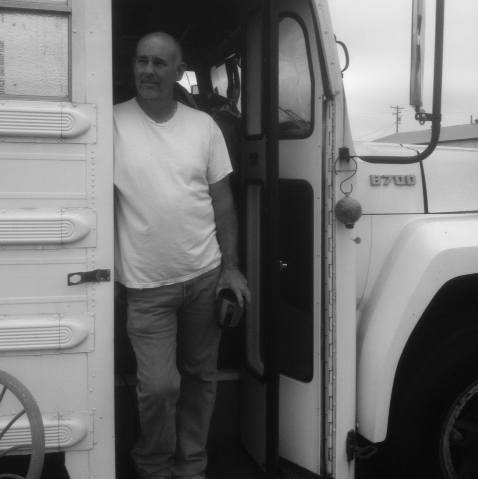
Wayne J Howell
age ~66
from Wappingers Falls, NY
- Also known as:
-
- Wayne John Howell
- Wayne S Howell
- Wayne John Murley
- Susan Howell
Wayne Howell Phones & Addresses
- Wappingers Falls, NY
- Lafayette, CO
- Fishkill, NY
- Schroon Lake, NY
- 1 Megans Cir, Newtown, CT 06470 • (203)3640230
- Poughkeepsie, NY
- Williston, VT
- South Burlington, VT
- Champaign, IL
- Wappingers Fl, NY
- Urbana, IL
Work
-
Position:Student
Education
-
Degree:High school graduate or higher
Emails
Us Patents
-
Rolling Ball Connector
view source -
US Patent:6358627, Mar 19, 2002
-
Filed:Jan 23, 2001
-
Appl. No.:09/768112
-
Inventors:Joseph A. Benenati - Hopewell Junction NY
Claude L. Bertin - South Burlington VT
William T. Chen - Endicott NY
Thomas E. Dinan - San Jose CA
Wayne F. Ellis - Jericho VT
Wayne J. Howell - Williston VT
John U. Knickerbocker - Hopewell Junction NY
Mark V. Pierson - Binghamton NY
William R. Tonti - Essex Junction NY
Jerzy M. Zalesinski - Essex Junction NY -
Assignee:International Business Machines Corporation - Armonk NY
-
International Classification:H01L 2144
-
US Classification:428612, 438613, 438666
-
Abstract:An integrated circuit assembly has pads of a chip electrically connected to pads of a substrate with rolling metal balls. A pliable material bonds the balls in movable contact with pads of the chip and substrate. Because the balls are relatively free to move, thermal expansion differences that would ordinarily cause enormous stresses in the attached joints of the prior art, simply cause rolling of the balls of the present invention, avoiding thermal stress altogether. Reliability of the connections is substantially improved as compared with C4 solder bumps, and chips can be safely directly mounted to such substrates as PC boards, despite substantial thermal mismatch.
-
Method For Forming Three-Dimensional Circuitization And Circuits Formed
view source -
US Patent:6426241, Jul 30, 2002
-
Filed:Nov 12, 1999
-
Appl. No.:09/439112
-
Inventors:Steven A. Cordes - Cortlandt Manor NY
Peter A. Gruber - Mohegan Lake NY
James L. Speidell - Poughquag NY
Wayne J. Howell - Williston VT
Thomas G. Ference - Essex Junction VT -
Assignee:International Business Machines Corporation - Armonk NY
-
International Classification:H01L 2144
-
US Classification:438108, 438124, 438126, 438127, 438637
-
Abstract:A method for forming three-dimensional circuitization in a substrate is provided for forming conductive traces and via contacts. In the method, a substrate formed of a substantially insulating material is first provided, grooves and apertures in a top surface of and through the substrate are then formed, followed by filling the grooves and apertures with an electrically conductive material such as a solder. The method can be carried out at a low cost to produce high quality circuit substrates by utilizing an injection molded solder technique or a molten solder screening technique to fill the grooves and the apertures. The grooves and the apertures in the substrate may be formed by a variety of techniques such as chemical etching, physical machining and hot stamping.
-
Semiconductor Structure And Package Including A Chip Having Chamfered Edges
view source -
US Patent:6600213, Jul 29, 2003
-
Filed:May 15, 2001
-
Appl. No.:09/855617
-
Inventors:Donald W. Brouillette - St. Albans VT
Robert F. Cook - Putnam Valley NY
Thomas G. Ference - Essex Junction VT
Wayne J. Howell - Williston VT
Eric G. Liniger - Danbury CT
Ronald L. Mendelson - Richmond VT -
Assignee:International Business Machines Corporation - Armonk NY
-
International Classification:H01L 2906
-
US Classification:257618, 257171, 257496, 257586, 257678
-
Abstract:A semiconductor structure with greatly reduced backside chipping and cracking, as well as increased die strength, accommodation of compact assembly with a carrier such as another semiconductor chip, and resistance to package damage is provided by dicing chips from a wafer in a manner that chamfers edges of the chips. Similar advantages are obtained in multi-chip structure.
-
Method And System For Dicing Wafers, And Semiconductor Structures Incorporating The Products Thereof
view source -
US Patent:6915795, Jul 12, 2005
-
Filed:May 30, 2003
-
Appl. No.:10/448305
-
Inventors:Donald W. Brouillette - St. Albans VT, US
Robert F. Cook - Putnam Valley NY, US
Thomas G. Ference - Essex Junction VT, US
Wayne J. Howell - Williston VT, US
Eric G. Liniger - Danbury CT, US
Ronald L. Mendelson - Richmond VT, US -
Assignee:International Business Machines Corporation - Armonk NY
-
International Classification:B28D001/04
-
US Classification:125 13, 125 12, 125 1301, 125 14, 125 15, 125 20, 451 6, 451 8, 451 9, 451 10
-
Abstract:A method and system for dicing a semiconductor wafer providing a structure with greatly reduced backside chipping and cracking, as well as increased die strength. Semiconductor chip structures obtained from wafers diced according to this invention are also encompassed.
-
Method For Forming Three-Dimensional Circuitization And Circuits Formed
view source -
US Patent:20020113324, Aug 22, 2002
-
Filed:Apr 24, 2002
-
Appl. No.:10/131803
-
Inventors:Steven Cordes - Cortlandt Manor NY, US
Peter Gruber - Mohegan Lake NY, US
James Speidell - Poughquag NY, US
Wayne Howell - Williston VT, US
Thomas Ference - Essex Junction VT, US -
Assignee:International Business Machines Corporation - Armonk NY
-
International Classification:H01L021/44
H01L023/48
H01L029/40
H01L023/52 -
US Classification:257/784000, 438/617000, 438/614000, 257/781000, 257/786000
-
Abstract:A method for forming three-dimensional circuitization in a substrate is provided for forming conductive traces and via contacts. In the method, a substrate formed of a substantially insulating material is first provided, grooves and apertures in a top surface of and through the substrate are then formed, followed by filling the grooves and apertures with an electrically conductive material such as a solder. The method can be carried out at a low cost to produce high quality circuit substrates by utilizing an injection molded solder technique or a molten solder screening technique to fill the grooves and the apertures. The grooves and the apertures in the substrate may be formed by a variety of techniques such as chemical etching, physical machining and hot stamping.
-
Underfill Preform Interposer For Joining Chip To Substrate
view source -
US Patent:62586270, Jul 10, 2001
-
Filed:Jan 19, 1999
-
Appl. No.:9/233388
-
Inventors:Joseph A. Benenati - Hopewell Junction NY
William T. Chen - Singapore, SG
Lisa A. Fanti - Hopewell Junction NY
Wayne J. Howell - Williston VT
John U. Knickerbocker - Hopewell Junction NY -
Assignee:International Business Machines Corporation - Armonk NY
-
International Classification:H01L 2144
H01L 2160 -
US Classification:438108
-
Abstract:An apparatus for and method of minimizing the thermo-mechanical fatigue of flip-chip packages. The interposer of the present invention, preferably comprising an organic polymer such as polyimide, contains apertures having conductive plugs inserted therein for joining a chip to a substrate in an electronic module utilizing flip-chip packaging. The interposer is selected to provide optimum spacing between the chip and substrate having a coefficient of thermal expansion adapted to the thermal cycling temperature extremes of the module components. The interposer may comprise an inner core with two adhesive outer layers which may comprise different materials to promote adhesion at their respective interfaces within a module. Conductive plugs are disposed within the apertures of the interposer comprising of a first and second solder or comprising a conductive plug having top and bottom surfaces coated with a conductive adhesive. Preferably, the first solder is disposed within an interior of the apertures and the second solder is disposed within an exterior of the apertures such that the first solder is between a first portion and a second portion of the second solder.
-
Method And System For Dicing Wafers, And Semiconductor Structures Incorporating The Products Thereof
view source -
US Patent:62711024, Aug 7, 2001
-
Filed:Feb 27, 1998
-
Appl. No.:9/032151
-
Inventors:Donald W. Brouillette - St. Albans VT
Robert F. Cook - Putnam Valley NY
Thomas G. Ference - Essex Junction VT
Wayne J. Howell - Williston VT
Eric G. Liniger - Danbury CT
Ronald L. Mendelson - Richmond VT -
Assignee:International Business Machines Corporation - Armonk NY
-
International Classification:H01L 21301
H01L 2146
H01L 2178
B26D 300
B26D 302
B26D 308 -
US Classification:438462
-
Abstract:A method and system for dicing a semiconductor wafer providing a structure with greatly reduced backside chipping and cracking, as well as increased die strength. Semiconductor chip structures obtained from wafers diced according to this invention are also encompassed.
Name / Title
Company / Classification
Phones & Addresses
Owner
Xtreme Renos & Construction Ltd.
Contractors - General. Fence Contractors. Windows - Installation & Service. Siding Contractors. Roofing Contractors. Roof Decks. Home Improvements. Garage Builders. Building Contractors
Contractors - General. Fence Contractors. Windows - Installation & Service. Siding Contractors. Roofing Contractors. Roof Decks. Home Improvements. Garage Builders. Building Contractors
66 Jordan Place, PO Box 662, Shea Heights, NL A0A 1J0
(709)7547366
(709)7547366
Owner
Xtreme Renos & Construction Ltd
Contractors - General · Fence Contractors · Windows - Installation & Service · Siding Contractors · Roofing Contractors · Roof Decks · Home Improvements · Garage Builders
Contractors - General · Fence Contractors · Windows - Installation & Service · Siding Contractors · Roofing Contractors · Roof Decks · Home Improvements · Garage Builders
(709)7547366
VP Engineering
The Beacon Institute Inc
Commercial Physical Research
Commercial Physical Research
199 Main St, Beacon, NY 12508
(845)8381600
(845)8381600
Resumes

Wayne Howell
view source
Wayne Howell
view source
Computer Specialist
view sourceWork:
Computer Specialist

Wayne Howell
view source
Wayne Howell
view source
Wayne Howell
view source
Wayne Howell
view source
Wayne Howell
view sourceYoutube
Flickr
Googleplus

Wayne Howell (Barkodeotb)
Lived:
Lakewood, CO
Shelby, NC
Killeen, TX
Shelby, NC
Killeen, TX
Work:
Coal Powered Media Group - Producer (2012)
About:
If you looking for a unique cinematic sound, then I'm your producer!
Tagline:
All Board With The Train. Let's get it!

Wayne Howell
Lived:
Newtown, CT
Education:
Clarkson University

Wayne Howell
Work:
Blue Trading Co - Owner
Tagline:
Husband, father, music lover, writer, poet, just another face in the crowd . . .

Wayne Howell
Education:
Bowie State University

Wayne “Dragonbloodsoup” H...

Wayne Howell

Wayne Howell

Wayne Howell
Plaxo

Wayne Howell
view sourceCharlotte

Wayne Howell
view source
Wayne Howell
view sourceAlgonquin, IL

Wayne Howell
view sourceBellSouth

Wayne Howell
view sourceResource Manager at TAKE Solutions

Wayne Howell
view source
Jathan Wayne Howell
view source
Wayne J Howell
view source
Elect Darrin D'Wayne Howell
view source
Wayne L. Howell Sr.
view source
Wayne Howell
view source
Wayne E. Howell
view source
Wayne W. Howell
view sourceClassmates

Wayne Hawkins (Howell)
view sourceSchools:
Altoona-Midway High School Buffalo KS 1957-1958
Community:
Steve Johnson, Mike Lucas, Karyn Adcock, Peggy Dewitt, Vickie Toon
Biography:
Still hanging around, hope the rest of you are still with us.
I always wanted to be ...

Wayne Howell
view sourceSchools:
Flathead High School Kalispell MT 1975-1979
Community:
Jessie Mccormick, Chip Anderson

Wayne Howell
view sourceSchools:
Buckskin Valley High School South Salem OH 1973-1977

Wayne Howell
view sourceSchools:
E.M. Lasert High School Edmonton Azores 1990-1997
Community:
Nicole Magnusson, Amber Anderson, Jaime Carson, Boch Choi, Rick Devoldere, Julie Sanders

Wayne Howell
view sourceSchools:
Chestnut Hills Elementary School Beltsville MD 1965-1971
Community:
Diedra Cowan, Nancy Burditt, Denise Vernon, Idonas Hughes, Deborah Hallameyer

Wayne Howell (Same)
view sourceSchools:
Jackson County High School Gainesboro TN 1955-1959

Wayne Howell
view sourceSchools:
Gonzaga High School St. John's Peru 1987-1991
Community:
Matt Gauci, Cathy Gillies, Darren Walker
Get Report for Wayne J Howell from Wappingers Falls, NY, age ~66


