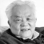
Wen Sheng Wu
age ~51
from Redlands, CA
- Also known as:
-
- Wen Ho Wu
- Wen H Wu
- Wen S Wu
- Wensheng Wu
- Wen-Ho Wu
- Sheng Wu Wensheng
Wen Wu Phones & Addresses
- Redlands, CA
- Cupertino, CA
- Rowland Heights, CA
- Parsippany, NJ
- Flushing, NY
- Rowland Heights, CA
- Montville, NJ
Real Estate Brokers

Wen Wu, Alhambra CA Realtor
view sourceSpecialties:
Buyer's Agent
Listing Agent
Listing Agent
Work:
Centry 21
115 S. Garfield Ave.,, Alhambra, CA 91801
(626)9458878 (Office)
115 S. Garfield Ave.,, Alhambra, CA 91801
(626)9458878 (Office)
Medicine Doctors

Dr. Wen Wu, Foster City CA - DDS (Doctor of Dental Surgery)
view sourceSpecialties:
Dentistry
Address:
1289 E Hillsdale Blvd Suite 9, Foster City, CA 94404
(650)6389688 (Phone), (650)6389689 (Fax)
(650)6389688 (Phone), (650)6389689 (Fax)
Languages:
English

Wen Shuo Wu, Whittier CA
view sourceSpecialties:
Acupuncture
Address:
16200 Amber Valley Dr, Whittier, CA 90604
(562)9437125 (Phone), (562)9023398 (Fax)
(562)9437125 (Phone), (562)9023398 (Fax)
Languages:
English
Name / Title
Company / Classification
Phones & Addresses
Owner
Wen Wu, DDS- Family Dental
Dentists
Dentists
1289 E. Hillsdale Blvd, Suite 9, Foster City, CA 94404-1294
(650)6389688, (650)6389689
(650)6389688, (650)6389689
President
XING LIN (USA) INTERNATIONAL CORP
Cotton Broadwoven Fabric Mill
Cotton Broadwoven Fabric Mill
1410 Broadway, New York, NY 10018
New Land Fashion 1410 Broadway STE 300, New York, NY 10018
1407 Broadway, New York, NY 10018
36 Milk Rd, Edison, NJ 08837
(212)9474846
New Land Fashion 1410 Broadway STE 300, New York, NY 10018
1407 Broadway, New York, NY 10018
36 Milk Rd, Edison, NJ 08837
(212)9474846
President
PRESIDENT ENTERPRISE INC
Commercial Printing
Commercial Printing
700 Columbia St, Brea, CA 92821
(714)6719577, (714)6719587
(714)6719577, (714)6719587
President
BV&H INTERNATIONAL CORP
Whol Men's/Boy's Clothing
Whol Men's/Boy's Clothing
14854 Donna St, San Leandro, CA 94578
(510)3510318
(510)3510318
President
REDMAN USA INC
Whol Furniture
Whol Furniture
15249 Don Julian Rd, Hacienda Heights, CA 91745
15249 Don Julian Rd, Whittier, CA 91745
15249 Don Julian Rd, Whittier, CA 91745
Owner
Wen Wu, DDS- Family Dental
Dentists
Dentists
1289 E Hillsdale Blvd SUITE 9, San Mateo, CA 94404
(650)6389688, (650)6389689
(650)6389688, (650)6389689
President
QUALIDENT, INC
1289 E Hillsdale Blvd STE 9, San Mateo, CA 94404
Principal
Frooogal Limited Liability Company
Nonclassifiable Establishments
Nonclassifiable Establishments
2 Meadowbrook Rd, Syosset, NY 11791
Isbn (Books And Publications)

Resumes

Wen Yi Wu
view source
Wen Hua Wu
view source
Wen Hsin Wu
view source
Wen Wu
view source
Wen Wu
view source
Wen Wu
view source
Wen Wu
view source
Clerk At Bnp Paribas
view sourcePosition:
clerk at BNP Paribas
Location:
United States
Industry:
Banking
Work:
BNP Paribas
clerk
clerk
Lawyers & Attorneys

Wen Wu, New York NY - Lawyer
view sourceAddress:
Skadden, Arps, Slate, Meagher & Flom LLP
4 Times Sq, New York, NY 10036
(212)7352166 (Office)
4 Times Sq, New York, NY 10036
(212)7352166 (Office)
Licenses:
New York - Currently registered 2004
Education:
Columbia

Wen Wu - Lawyer
view sourceOffice:
McGraw Hill Financial, Inc.
Specialties:
Securitization
Structured Finance
Structured Finance
ISLN:
917605114
Admitted:
2004
University:
Beijing Foreign Studies University, Beijing, China, B.A., 1997; Northwestern University, M.A., 1999
Law School:
Columbia University, J.D., 2003
Us Patents
-
Compositionally Graded Titanium Nitride Film For Diffusion Barrier Applications
view source -
US Patent:7727882, Jun 1, 2010
-
Filed:Dec 17, 2007
-
Appl. No.:12/002780
-
Inventors:Wen Wu - Milpitas CA, US
Chentao Yu - Sunnyvale CA, US
Girish Dixit - San Jose CA, US
Kenneth Jow - San Jose CA, US -
Assignee:Novellus Systems, Inc. - San Jose CA
-
International Classification:H01L 21/4763
-
US Classification:438627, 438625, 438643, 438656, 438675, 438685, 257E21584
-
Abstract:A diffusion barrier film includes a layer of compositionally graded titanium nitride, having a nitrogen-rich portion and a nitrogen-poor portion. The nitrogen-rich portion has a composition of at least about 40% (atomic) N, and resides closer to the dielectric than the nitrogen-poor portion. The nitrogen-poor portion has a composition of less than about 30% (atomic) N (e. g. , between about 5-30% N) and resides in contact with the metal, e. g. , copper. The diffusion barrier film can also include a layer of titanium residing between the layer of dielectric and the layer of compositionally graded titanium nitride. The layer of titanium is often partially or completely converted to titanium oxide upon contact with a dielectric layer. The barrier film having a compositionally graded titanium nitride layer provides excellent diffusion barrier properties, exhibits good adhesion to copper, and reduces uncontrolled diffusion of titanium into interconnects.
-
Portion Of A Clock
view source -
US Patent:D621725, Aug 17, 2010
-
Filed:Mar 10, 2010
-
Appl. No.:29/357289
-
Inventors:Wen Chen Wu - Port Washington NY, US
-
Assignee:Kirch Industrial Co (USA) Ltd. - Farmingdale NY
-
International Classification:1001
-
US Classification:D10 20
-
Deposition Of Doped Copper Seed Layers Having Improved Reliability
view source -
US Patent:8017523, Sep 13, 2011
-
Filed:May 16, 2008
-
Appl. No.:12/122118
-
Inventors:Hui-Jung Wu - Fremont CA, US
Daniel R. Juliano - Santa Clara CA, US
Wen Wu - San Jose CA, US
Girish Dixit - San Jose CA, US -
Assignee:Novellus Systems, Inc. - San Jose CA
-
International Classification:H01L 21/4763
-
US Classification:438687, 438627, 438675, 438678
-
Abstract:Improved methods of depositing copper seed layers in copper interconnect structure fabrication processes are provided. Also provided are the resulting structures, which have improved electromigration performance and reduced line resistance. According to various embodiments, the methods involve depositing a copper seed bilayer on a barrier layer in a recessed feature on a partially fabricated semiconductor substrate. The bilayer has a copper alloy seed layer and a pure copper seed layer, with the pure copper seed layer is deposited on the copper alloy seed layer. The copper seed bilayers have reduced line resistance increase and better electromigration performance than conventional doped copper seed layers. Precise line resistance control is achieved by tuning the bilayer thickness to meet the desired electromigration performance.
-
Device For Displaying Real Time And Advertising Media
view source -
US Patent:8018797, Sep 13, 2011
-
Filed:Nov 10, 2006
-
Appl. No.:11/595032
-
Inventors:Wen Chen Wu - Port Washington NY, US
-
International Classification:G04B 19/24
G04B 37/12
G09D 3/04 -
US Classification:368 41, 368278, 40121
-
Abstract:The present invention is a device for displaying real time and advertising media to a person. In one embodiment, the device comprises a front cover, a clock engaged with said front cover for displaying real time, and a first sheet having an advertising portion. The first sheet is moveably engaged with the front cover to an open position where the real time and advertising portion are visible to the person. The clock comprises a clock movement mechanism engaged with the front cover, a clock face imprinted on the front cover, and an hour and minute hand engaged with the clock movement mechanism. The device further comprises a mounting fastener engaged with front cover and clock movement mechanism. The mounting fastener is adapted to allow the device to be hung on a wall.
-
Resistive Switching Memory Element Including Doped Silicon Electrode
view source -
US Patent:8183553, May 22, 2012
-
Filed:Oct 29, 2009
-
Appl. No.:12/608934
-
Inventors:Prashant Phatak - San Jose CA, US
Tony Chiang - Campbell CA, US
Michael Miller - San Jose CA, US
Wen Wu - Pleasanton CA, US -
Assignee:Intermolecular, Inc. - San Jose CA
-
International Classification:H01L 47/00
-
US Classification:257 4, 257E45003, 365148
-
Abstract:A resistive switching memory element including a doped silicon electrode is described, including a first electrode comprising doped silicon having a first work function, a second electrode having a second work function that is different from the first work function by between 0. 1 and 1. 0 electron volts (eV), a metal oxide layer between the first electrode and the second electrode, the metal oxide layer switches using bulk-mediated switching and has a bandgap of greater than 4 eV, and the memory element switches from a low resistance state to a high resistance state and vice versa.
-
Nonvolatile Memory Element Including Resistive Switching Metal Oxide Layers
view source -
US Patent:8294219, Oct 23, 2012
-
Filed:Jul 24, 2008
-
Appl. No.:12/179538
-
Inventors:Sandra G. Malhotra - San Jose CA, US
Pragati Kumar - Santa Clara CA, US
Sean Barstow - San Jose CA, US
Tony Chiang - Campbell CA, US
Prashant B. Phatak - San Jose CA, US
Wen Wu - Pleasanton CA, US
Sunil Shanker - Santa Clara CA, US -
Assignee:Intermolecular, Inc. - San Jose CA
-
International Classification:H01L 21/02
-
US Classification:257382, 257 68, 257296, 257 71, 257309, 257905, 257908, 257E27084, 257E27075, 257E27097, 257758, 257308
-
Abstract:Nonvolatile memory elements that are based on resistive switching memory element layers are provided. A nonvolatile memory element may have a resistive switching metal oxide layer. The resistive switching metal oxide layer may have one or more layers of oxide. A resistive switching metal oxide may be doped with a dopant that increases its melting temperature and enhances its thermal stability. Layers may be formed to enhance the thermal stability of the nonvolatile memory element. An electrode for a nonvolatile memory element may contain a conductive layer and a buffer layer.
-
Charge Blocking Layers For Nonvolatile Memories
view source -
US Patent:8298890, Oct 30, 2012
-
Filed:Sep 3, 2009
-
Appl. No.:12/553918
-
Inventors:Ronald John Kuse - Dublin CA, US
Monica Sawkar Mathur - San Jose CA, US
Wen Wu - Pleasanton CA, US -
Assignee:Intermolecular, Inc. - San Jose CA
-
International Classification:H01L 21/336
-
US Classification:438257, 438211, 438593, 438972, 257239, 257261, 257298, 257E21179, 257E21495
-
Abstract:A semiconductor memory element is described, including a substrate including a source region, a drain region, and a channel region, a tunnel oxide over the channel region of the substrate, a charge storage layer over the tunnel oxide, a charge blocking layer over the charge storage layer, and a control gate over the charge blocking layer. The charge blocking layer further includes a first layer including a transition metal oxide, a second layer including a metal silicate, a third layer including the transition metal oxide of the first layer.
-
Nonvolatile Memory Elements
view source -
US Patent:8318573, Nov 27, 2012
-
Filed:Dec 27, 2011
-
Appl. No.:13/337611
-
Inventors:Sandra G. Malhotra - San Jose CA, US
Pragati Kumar - Santa Clara CA, US
Sean Barstow - San Jose CA, US
Tony Chiang - Campbell CA, US
Prashant B. Phatak - San Jose CA, US
Wen Wu - Pleasanton CA, US
Sunil Shanker - Santa Clara CA, US -
Assignee:Intermolecular, Inc. - San Jose CA
-
International Classification:H01L 21/02
-
US Classification:438382, 257E21004, 257E27084, 257E27075, 257E27097, 257 68, 257296
-
Abstract:Nonvolatile memory elements that are based on resistive switching memory element layers are provided. A nonvolatile memory element may have a resistive switching metal oxide layer. The resistive switching metal oxide layer may have one or more layers of oxide. A resistive switching metal oxide may be doped with a dopant that increases its melting temperature and enhances its thermal stability. Layers may be formed to enhance the thermal stability of the nonvolatile memory element. An electrode for a nonvolatile memory element may contain a conductive layer and a buffer layer.
Youtube
Googleplus

Wen Wu
Education:
Peking University - Economics, Peking University - EECS
Tagline:
Me is me, mine is mine!

Wen Wu

Wen Wu
Bragging Rights:
台灣靜心發展協會理事長

Wen Wu
Education:
University of Exeter - Finance and management

Wen Wu

Wen Wu

Wen Wu

Wen Wu
Flickr
Myspace
Plaxo

Wen Wu
view sourceLaurentian University

Wen Tsun Wu
view source
Wen Wu
view source
Wen Wu
view source
Wen Quian Wu
view source
Wen Qing Wu
view source
Wen Zhong Wu
view source
Wen Shin Wu
view source
Guan Wen Wu
view sourceClassmates
Get Report for Wen Sheng Wu from Redlands, CA, age ~51


