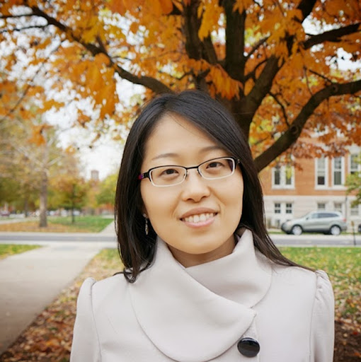
Xin Chen
age ~44
from Chino, CA
- Also known as:
-
- Xi N Chen
Xin Chen Phones & Addresses
- Chino, CA
- 6102 City Shores Ln, Katy, TX 77494
- Richmond, TX
- Houston, TX
- Stillwater, OK
- San Francisco, CA
- Discovery Bay, CA
Isbn (Books And Publications)

Logic of Logistics: Theory, Algorithms, and Applications for Logistics Management
view sourceAuthor
Xin Chen
ISBN #
0387221999

Medicine Doctors

Xin Qian Chen
view sourceSpecialties:
Physical Medicine & Rehabilitation
Work:
Aurora Medical GroupAurora Baycare Medical Center
2845 Greenbrier Rd, Green Bay, WI 54311
(920)2888000 (phone), (920)2885510 (fax)
Bay Care Clinic Physical Medicine
2845 Greenbrier Rd STE 340, Green Bay, WI 54311
(920)2888377 (phone), (920)2888385 (fax)
2845 Greenbrier Rd, Green Bay, WI 54311
(920)2888000 (phone), (920)2885510 (fax)
Bay Care Clinic Physical Medicine
2845 Greenbrier Rd STE 340, Green Bay, WI 54311
(920)2888377 (phone), (920)2888385 (fax)
Education:
Medical School
The Fourth Military Med Univ, Xian City, Shaanxi, China
Graduated: 1984
The Fourth Military Med Univ, Xian City, Shaanxi, China
Graduated: 1984
Procedures:
Physical Medicine and Rehabilitation, Tests and Measurements
Physical Therapy
Physical Therapy Evaluation
Arthrocentesis
Neurological Testing
Physical Therapy
Physical Therapy Evaluation
Arthrocentesis
Neurological Testing
Conditions:
Cholelethiasis or Cholecystitis
Gastrointestinal Hemorrhage
Inguinal Hernia
Malignant Neoplasm of Esophagus
Varicose Veins
Gastrointestinal Hemorrhage
Inguinal Hernia
Malignant Neoplasm of Esophagus
Varicose Veins
Languages:
Chinese
English
French
Spanish
English
French
Spanish
Description:
Dr. Chen graduated from the The Fourth Military Med Univ, Xian City, Shaanxi, China in 1984. He works in Green Bay, WI and 1 other location and specializes in Physical Medicine & Rehabilitation. Dr. Chen is affiliated with Aurora Baycare Medical Center.

Xin Chen
view sourceSpecialties:
Pediatrics
Work:
TJH Medical Services PCTJH Medical Services
9229 Queens Blvd STE C1, Rego Park, NY 11374
(718)5751992 (phone), (917)8326697 (fax)
9229 Queens Blvd STE C1, Rego Park, NY 11374
(718)5751992 (phone), (917)8326697 (fax)
Education:
Medical School
Peking Union Med Coll, Beijing, Beijing, China
Graduated: 1993
Peking Union Med Coll, Beijing, Beijing, China
Graduated: 1993
Conditions:
Acute Bronchitis
Acute Conjunctivitis
Acute Pharyngitis
Acute Sinusitis
Acute Upper Respiratory Tract Infections
Acute Conjunctivitis
Acute Pharyngitis
Acute Sinusitis
Acute Upper Respiratory Tract Infections
Languages:
Chinese
English
Spanish
English
Spanish
Description:
Dr. Chen graduated from the Peking Union Med Coll, Beijing, Beijing, China in 1993. She works in Rego Park, NY and specializes in Pediatrics. Dr. Chen is affiliated with Flushing Hospital Medical Center and Jamaica Hospital Medical Center.
Name / Title
Company / Classification
Phones & Addresses
President
Myscenery International Private Vacation Club Co., Ltd
1313 N Grand Ave, Walnut, CA 91789
President
CALIFORNIA EASY TRADING INC
Whol Nondurable Goods
Whol Nondurable Goods
5931 Rowland Ave, Temple City, CA 91780
5460 Peck Rd, Arcadia, CA 91006
5460 Peck Rd, Arcadia, CA 91006
President
BRIGHT WISH, INC
Nonclassifiable Establishments
Nonclassifiable Establishments
457 W Allen Ave STE #115, San Dimas, CA 91773
20468 Carrey Rd, Walnut, CA 91789
17959 Ajax Cir, Whittier, CA 91748
750 W Walnut Ave, Monrovia, CA 91016
20468 Carrey Rd, Walnut, CA 91789
17959 Ajax Cir, Whittier, CA 91748
750 W Walnut Ave, Monrovia, CA 91016
Principal
Easy Trading Inc
Whol Nondurable Goods
Whol Nondurable Goods
5931 Rowland Ave, Temple City, CA 91780
Director, President, Secretary, Treasurer
Flm Minerals Inc
Chairman, Secretary
OPAL PARKER ELECTRIC LLC
3775 Medlock Brg Rd, Norcross, GA 30092
3592 Rosemead Blvd, Rosemead, CA 91770
3592 Rosemead Blvd, Rosemead, CA 91770
SANHE INC
UM CONSULTING CLEVELAND, INC
Us Patents
-
Thin Film Solid Oxide Fuel Cell And Method For Forming
view source -
US Patent:6645656, Nov 11, 2003
-
Filed:Mar 24, 2000
-
Appl. No.:09/534385
-
Inventors:Xin Chen - Houston TX
Naijuan Wu - Houston TX
Alex Ignatiev - Houston TX -
Assignee:University of Houston - Houston TX
-
International Classification:H01M 810
-
US Classification:429 32, 429 30, 429 33
-
Abstract:A thin film solid oxide fuel cell (TFSOFC) having a porous metallic anode and a porous cathode is provided. The fuel cell is formed by using a continuous metal foil as a substrate to epitaxially deposit a thin film electrolyte on one surface of the foil. The metal foil may then be made porous by photolithographically patterning and etching the other surface of the foil to form holes extending through the foil to the electrolyte/foil interface. The cathode is then formed on the electrolyte by depositing a second thin film using known film deposition techniques. Further processing may be used to increase the porosity of the electrodes. The metal foil may be treated before film deposition to have an atomically ordered surface, which makes possible an atomically ordered thin film electrolyte.
-
Thin Film Solid Oxide Fuel Cell And Method For Forming
view source -
US Patent:7381492, Jun 3, 2008
-
Filed:Nov 10, 2003
-
Appl. No.:10/704725
-
Inventors:Xin Chen - Houston TX, US
Naijuan Wu - Pearland TX, US
Alex Ignatiev - Houston TX, US -
Assignee:University of Houston - Houston TX
-
International Classification:H01M 8/10
B05D 5/12 -
US Classification:429 30, 427115
-
Abstract:A thin film solid oxide fuel cell (TFSOFC) having a porous metallic anode and a porous cathode is provided. The fuel cell is formed by using a continuous metal foil as a substrate to epitaxially deposit a thin film electrolyte on one surface of the foil. The metal foil may then be made porous by photolithographically patterning and etching the other surface of the foil to form holes extending through the foil to the electrolyte/foil interface. The cathode is then formed on the electrolyte by depositing a second thin film using known film deposition techniques. Further processing may be used to increase the porosity of the electrodes. The metal foil may be treated before film deposition to have an atomically ordered surface, which makes possible an atomically ordered thin film electrolyte.
-
Thin Film Solid Oxide Fuel Cell With Lithographically Patterned Electrolyte And Anode Layers
view source -
US Patent:7510819, Mar 31, 2009
-
Filed:May 18, 2006
-
Appl. No.:11/436392
-
Inventors:Xin Chen - Houston TX, US
Naijuan Wu - Houston TX, US
Alex Ignatiev - Houston TX, US
Yuxiang Zhou - Houston TX, US -
Assignee:Board of Regents, University of Houston - Houston TX
-
International Classification:B05D 5/12
H01M 4/88 -
US Classification:430320, 429100, 429159, 502101, 427115
-
Abstract:A thin film solid oxide fuel cell (TFSOFC) having a porous metallic anode and a porous cathode is provided. The fuel cell is formed by using a continuous metal foil as a substrate onto which is deposited a thin anode metal layer which is then patterned to reveal an array of pores in the anode. A dense thin film electrolyte is then deposited onto the porous anode layer overcoating the anode and filling the anode pores. The substrate foil layer is then removed to allow for exposure of the porous anode/electrolyte to fuel. The cathode is then formed on the electrolyte by depositing a cathode thin film cap using known film deposition techniques. Further processing may be used to increase the porosity of the electrodes. The metal foil may be treated to have an atomically ordered surface, which makes possible an atomically ordered anode and atomically ordered thin film electrolyte for improved performance.
-
Switchable Resistive Perovskite Microelectronic Device With Multi-Layer Thin Film Structure
view source -
US Patent:7608467, Oct 27, 2009
-
Filed:Jan 13, 2005
-
Appl. No.:11/034695
-
Inventors:Naijuan Wu - Houston TX, US
Xin Chen - Houston TX, US
Alex Ignatiev - Houston TX, US -
Assignee:Board of Regents University of Houston - Houston TX
-
International Classification:H01L 21/00
H01L 29/76 -
US Classification:438 3, 257295
-
Abstract:A switchable resistive device has a multi-layer thin film structure interposed between an upper conductive electrode and a lower conductive electrode. The multi-layer thin film structure comprises a perovskite layer with one buffer layer on one side of the perovskite layer, or a perovskite layer with buffer layers on both sides of the perovskite layer. Reversible resistance changes are induced in the device under applied electrical pulses. The resistance changes of the device are retained after applied electric pulses. The functions of the buffer layer(s) added to the device include magnification of the resistance switching region, reduction of the pulse voltage needed to switch the device, protection of the device from being damaged by a large pulse shock, improvement of the temperature and radiation properties, and increased stability of the device allowing for multivalued memory applications.
-
Method Of Using A Switchable Resistive Perovskite Microelectronic Device With Multi-Layer Thin Film Structure
view source -
US Patent:7955871, Jun 7, 2011
-
Filed:Sep 17, 2009
-
Appl. No.:12/586143
-
Inventors:Naijuan Wu - Houston TX, US
Xin Chen - Houston TX, US
Alex Ignatiev - Houston TX, US -
Assignee:Board of Regents, University of Houston - Houston TX
-
International Classification:H01L 21/00
H01L 29/76 -
US Classification:438 3, 257295
-
Abstract:A switchable resistive device has a multi-layer thin film structure interposed between an upper conductive electrode and a lower conductive electrode. The multi-layer thin film structure comprises a perovskite layer with one buffer layer on one side of the perovskite layer, or a perovskite layer with buffer layers on both sides of the perovskite layer. Reversible resistance changes are induced in the device under applied electrical pulses. The resistance changes of the device are retained after applied electric pulses. The functions of the buffer layer(s) added to the device include magnification of the resistance switching region, reduction of the pulse voltage needed to switch the device, protection of the device from being damaged by a large pulse shock, improvement of the temperature and radiation properties, and increased stability of the device allowing for multivalued memory applications.
-
Switchable Two Terminal Multi-Layer Perovskite Thin Film Resistive Device And Methods Thereof
view source -
US Patent:8089111, Jan 3, 2012
-
Filed:Sep 17, 2009
-
Appl. No.:12/586147
-
Inventors:Naijuan Wu - Houston TX, US
Xin Chen - Houston TX, US
Alex Ignatiev - Houston TX, US -
Assignee:Board of Regents, University of Houston - Houston TX
-
International Classification:H01L 29/76
H01L 21/00 -
US Classification:257295, 438 3
-
Abstract:A switchable resistive device has a multi-layer thin film structure interposed between an upper conductive electrode and a lower conductive electrode. The multi-layer thin film structure comprises a perovskite layer with one buffer layer on one side of the perovskite layer, or a perovskite layer with buffer layers on both sides of the perovskite layer. Reversible resistance changes are induced in the device under applied electrical pulses. The resistance changes of the device are retained after applied electric pulses. The functions of the buffer layer(s) added to the device include magnification of the resistance switching region, reduction of the pulse voltage needed to switch the device, protection of the device from being damaged by a large pulse shock, improvement of the temperature and radiation properties, and increased stability of the device allowing for multivalued memory applications.
-
Method Of Using A Buffered Electric Pulse Induced Resistance Device
view source -
US Patent:8409879, Apr 2, 2013
-
Filed:May 23, 2011
-
Appl. No.:13/068884
-
Inventors:Naijuan Wu - Houston TX, US
Xin Chen - Houston TX, US
Alex Ignatiev - Houston TX, US -
Assignee:Board of Regents, University of Houston - Houston TX
-
International Classification:H01L 21/00
H01L 21/02 -
US Classification:438 3, 257295
-
Abstract:A switchable resistive device has a multi-layer thin film structure interposed between an upper conductive electrode and a lower conductive electrode. The multi-layer thin film structure comprises a perovskite layer with one buffer layer on one side of the perovskite layer, or a perovskite layer with buffer layers on both sides of the perovskite layer. Reversible resistance changes are induced in the device under applied electrical pulses. The resistance changes of the device are retained after applied electric pulses. The selected duration of the electrical pulse is in the range of from about 8 nanosecond to about 100 milliseconds. The selected maximum value of the electrical pulse is in the range of from about 1 V to about 150 V. The electrical pulse may have square, saw-toothed, triangular, sine, oscillating or other waveforms, and may be of positive or negative polarity.
-
Biaxially Textured Single Buffer Layer For Superconductive Articles
view source -
US Patent:20040157747, Aug 12, 2004
-
Filed:Feb 10, 2003
-
Appl. No.:10/364908
-
Inventors:Xin Chen - Houston TX, US
Naijuan Wu - Pearland TX, US
Alex Ignatiev - Houston TX, US
Yimin Chen - Bridgewater NJ, US -
Assignee:THE UNIVERSITY OF HOUSTON SYSTEM
-
International Classification:B32B001/00
H01F006/00
H01B012/00
H01L039/00 -
US Classification:505/238000
-
Abstract:A thick atomically ordered single buffer layer for use in the integration of high temperature superconductor films with metallic substrates is disclosed. The buffer layer is a doped cerium oxide (CeO) material, where the doping reduces layer cracking through the modification of thermal expansion coefficient and film strain properties, while adjusting chemical properties and lattice parameters to better match those of the substrate and HTS layer.
Resumes

Xin Chen Tucson, AZ
view sourceWork:
Landy Energy Services Inc.
Sealy, TX
Jun 2014 to Aug 2014
Accounting Intern KPMG
Jul 2013 to Aug 2013
Audit Intern PricewaterhouseCoopers LLP
Jan 2011 to Feb 2011
Audit Intern
Sealy, TX
Jun 2014 to Aug 2014
Accounting Intern KPMG
Jul 2013 to Aug 2013
Audit Intern PricewaterhouseCoopers LLP
Jan 2011 to Feb 2011
Audit Intern
Education:
The University of Arizona
Tucson, AZ
2013 to 2014
Master of Science in Accounting China University of Petroleum
2008 to 2012
Bachelor of Administration in Accounting
Tucson, AZ
2013 to 2014
Master of Science in Accounting China University of Petroleum
2008 to 2012
Bachelor of Administration in Accounting
Skills:
SAP, QuickBooks, Microsoft Word, Excel, Outlook, and Access.

Xin Chen Houston, TX
view sourceWork:
Global Airworks
Industry, CA
Oct 2011 to Dec 2011
Internship
Industry, CA
Oct 2011 to Dec 2011
Internship
Education:
Rice University
Houston, TX
2013 to 2014
Master of Computer Engineering
Houston, TX
2013 to 2014
Master of Computer Engineering

Xin "Sunny" Chen San Francisco, CA
view sourceWork:
Kaiser Permanente
San Francisco, CA
Nov 2011 to Nov 2011
intern pharmacist Chinatown Public Health Center,
San Francisco, CA
Nov 2011 to Nov 2011
intern pharmacist Arlington Pharmacy
Arlington, CA
Mar 2010 to May 2011
Pharmacy Clerk, Kang Kang Pharmacy
Monterey Park, CA
Jun 2010 to Aug 2010
Pharmacy Technician & Clerk, E&J Pharmacy,
Alhambra, CA
May 2010 to Aug 2010
Pharmacy Technician Emerson Elementary School
Berkeley, CA
Mar 2010 to Jun 2010
mentor University of California, Berkeley
berkleey
Jan 2010 to May 2010
Honor Research Member Pasadena City College
Pasadena, TX
Jun 2008 to Jun 2009
Math and Chemistry Tutor Tzu Chi Free Clinic
Alhambra, CA
Jun 2007 to Jun 2009
Clinic Registrar Chinese Elementary School,
Alhambra, CA
Chinese totor
San Francisco, CA
Nov 2011 to Nov 2011
intern pharmacist Chinatown Public Health Center,
San Francisco, CA
Nov 2011 to Nov 2011
intern pharmacist Arlington Pharmacy
Arlington, CA
Mar 2010 to May 2011
Pharmacy Clerk, Kang Kang Pharmacy
Monterey Park, CA
Jun 2010 to Aug 2010
Pharmacy Technician & Clerk, E&J Pharmacy,
Alhambra, CA
May 2010 to Aug 2010
Pharmacy Technician Emerson Elementary School
Berkeley, CA
Mar 2010 to Jun 2010
mentor University of California, Berkeley
berkleey
Jan 2010 to May 2010
Honor Research Member Pasadena City College
Pasadena, TX
Jun 2008 to Jun 2009
Math and Chemistry Tutor Tzu Chi Free Clinic
Alhambra, CA
Jun 2007 to Jun 2009
Clinic Registrar Chinese Elementary School,
Alhambra, CA
Chinese totor
Education:
University of California
Berkeley, CA
May 2011
Bachelor of Science in Chemical Biology University of California
San Francisco, CA
Doctor of Pharmacy
Berkeley, CA
May 2011
Bachelor of Science in Chemical Biology University of California
San Francisco, CA
Doctor of Pharmacy
Skills:
Language: Proficient in Chinese (Mandarin) Trainings: Vaccination, Immunization, Aseptic Skills, Blood Glucose and Blood Pressure Screening, Hepatitis B Phlebotomy and Vaccination, CPR, Smoking Cessation, Medicare Part D

Xin Chen Simi Valley, CA
view sourceWork:
Riot Games, Inc
Jan 2012 to Present
Director of Accounting Source Photonics, Inc
Chatsworth, CA
Mar 2010 to Dec 2011
Director of Technical Accounting Volt Information Sciences Inc
Orange, CA
Apr 2009 to Mar 2010
Internal Audit Manager Ernst & Young LLP
San Jose, CA
Jul 2004 to Apr 2009
Audit Manager, Advisory & Assurance Business Services M. Green and Company LLP
Visalia, CA
Sep 2002 to May 2004
CPA Japan Tobacco
HK, HK
Sep 1997 to Aug 2000
Assistant Manager
Education:
California State University
Dec 2002
Master of Business Administration in Finance Hubei University
Jun 1993
Bachelor of Arts in English
Dec 2002
Master of Business Administration in Finance Hubei University
Jun 1993
Bachelor of Arts in English
Lawyers & Attorneys

Xin Chen - Lawyer
view sourceAddress:
Shearman & Sterling
(297)88001xx (Office)
(297)88001xx (Office)
Licenses:
New York - Currently registered 2002
Education:
Columbia University School of Law

Xin Chen - Lawyer
view sourceOffice:
The Law Offices of Xin Chen, PC
Specialties:
General Practice
International Law
Corporate Law
International Law
Corporate Law
ISLN:
915020056
Admitted:
2003
Law School:
College of William and Mary, LL.M., 1995; Indiana University-Indianapolis, J.D., 2002; Peking University, LL.B., 1982
Plaxo

chen xin
view source
Xin Chen
view sourceSanta Clara, CA

Xin Chen
view sourceSinoprogress

Chen Xin
view sourcePast: VITM at Atos Origin

Xin Yao Chen
view source
Xin Wei Chen
view source
Xin Yi Chen
view source
Xin Lei Chen
view source
Xin Sophie Chen
view source
Xin Xin Chen
view source
Xin Yao Chen
view source
Xin Ying Chen
view sourceYoutube
Classmates

Xin Chen
view sourceSchools:
Shenyang Yucai School High School Shenyang China 1990-1994
Community:
Teresa Schnell, Glen Robinson

Xin Chen
view sourceSchools:
purdue univers West Lafayette IN 2000-2002
Community:
Lamar Jones, Brecke Kelley, Terri Malone

Xin Chen
view sourceSchools:
Xiangmin High School Shanghai China 1982-1986
Community:
Glenda Case, Raazia Bokhari

Xin Chen
view sourceSchools:
Montauk Elementary School Montauk NY 1999-2003
Community:
Gerald Clark, Debbie Morici

Xin Chen
view sourceSchools:
Ft. Worth Country Day Ft. Worth TX 1999-2003
Community:
Tiffany Marable, Heather Davis

Xin Chen
view sourceSchools:
Edward B. Shallow Junior High School 227 Brooklyn NY 1999-2003
Community:
Carol Iannone, Lucille Epifania, Carole Martino

Jian-Xin Chen, El Monte H...
view source
Xin Chen | Edinboro Unive...
view sourceNews

Graphene Oxide: Nano-Warrior Reduces the Toxicity of Alzheimer's Proteins
view source- The next step is to investigate whether it is possible to develop a drug delivery system based on graphene oxide for Alzheimers disease, says Xin Chen. We also want to test whether graphene oxide has beneficial effects in additional models of neurodegenerative diseases, such as Parkinsons diseaReference: Graphene Oxide Attenuates Toxicity of Amyloid- Aggregates in Yeast by Promoting Disassembly and Boosting Cellular Stress Response by Xin Chen, Santosh Pandit, Lei Shi, Vaishnavi Ravikumar, Julie Bonne Khler, Ema Svetlicic, Zhejian Cao, Abhroop Garg, Dina Petranovic and Ivan Mijakovic,
- Date: Oct 04, 2023
- Category: Health
- Source: Google

Cells Get a Makeover, Cancer Follows: A Path to New Therapies or Warning to ...
view source- In this case, two young scientists, Holger Willenbring and Xin Chen, were trying to study a deadly, and fairly common, form of liver cancer called hepatocellular carcinoma. Chen and her group hoped to induce the cancer by activating oncogenes, genes that trigger cancer, in a group of liver cells cal
- Date: Jul 18, 2012
- Category: Health
- Source: Google

Jellyfish-Inspired Robot Runs on Hydrogen
view source- Although the components have each been reported before, "It is probably one of the first and best demonstrations of a combination of nanotechology, hydrogen-fuel technology and soft robotics," said Xin Chen of Boston University who was not a part of the study.
- Date: Mar 21, 2012
- Category: Sci/Tech
- Source: Google
Myspace
Flickr
Googleplus

Xin Chen
Work:
Bloomberg L.P. - Financial Software Developer (6)
FX Aliance LLC - Software Developer Intern (1-4)
Coverago LLC - Software Engineer Intern (4-7)
FX Aliance LLC - Software Developer Intern (1-4)
Coverago LLC - Software Engineer Intern (4-7)
Education:
Columbia University - Computer Science, Zhejiang University - Information Science and Engineering

Xin Chen
Work:
Terminator skynet - Eliminator (2090-3015)
Skynet
Skynet
Education:
Sint-montfortcollege
Tagline:
I'm the chinese eliminator

Xin Chen
Work:
TrendSource - Marketing Associate (2011)
Education:
San Diego State University - Marketing, Grossmont College - Business Administration
Tagline:
Dream Flighter!

Xin Chen
Education:
Duke University - Master of Economics, Miami University - Business Economics
About:
Disciple of Love and Beauty.Defender of Rationality and Humanity.

Xin Chen
Work:
COMODO - QA Engineer (2009)
Education:
Beijing Jiaotong University - Electromagnetic Compatibility, Beijing Jiaotong University - Optics

Xin Chen
Education:
Pennsylvania State University - CSE, Nanjing University - CS, None

Xin Chen
Education:
Purdue University
About:
I am currently a PhD student in the School of Engineering Education at Purdue University. I have a BS in Electrical Engineering. My research focuses on Social Media Analytics in the context of enginee...
Bragging Rights:
I like cooking and beautiful food; I think friends are very important in life.

Xin Chen
Work:
Chin Chin - Hostess
Education:
The Hague University - International Law
Tagline:
Carpe diem bitches
Get Report for Xin Chen from Chino, CA, age ~44


