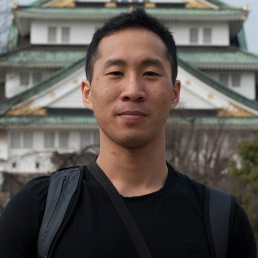
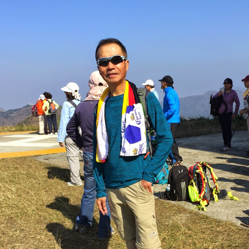
Paul Q Tsang
age ~56
from San Jose, CA
- Also known as:
-
- Paul Quang Tsang
- Paul A Tsang
- Paul O Tsang
- Paul Q Phang
- Tuong Q Tran
- Paul O'Tsang
- Tai Q Tran
- Thai Tran
- Than Tran
- Tran Toung
- Phone and address:
-
446 Chilberg Ct, San Jose, CA 95133
(408)2645818
Paul Tsang Phones & Addresses
- 446 Chilberg Ct, San Jose, CA 95133 • (408)2645818 • (408)8918981
- Santa Clara, CA
Work
-
Company:Masterpiece portrait & wedding
-
Address:1160 El Camino Real, San Carlos, CA 94070
-
Phones:(650)5933634
-
Position:Owner
-
Industries:Photographic Studios, Portrait
Us Patents
-
Method For Manufacturing Field Effect Transistors
view source -
US Patent:44425899, Apr 17, 1984
-
Filed:Mar 5, 1981
-
Appl. No.:6/240677
-
Inventors:Ven Y. Doo - San Jose CA
Paul J. Tsang - Poughkeepsie NY -
Assignee:International Business Machines Corporation - Armonk NY
-
International Classification:H01L 21265
H01L 2128 -
US Classification:29571
-
Abstract:A transistor and method of forming the same are disclosed. A thick mesa of dielectric material is grown on a semiconductor substrate and two or more layers of polycrystalline silicon grown on the vertical sides of the mesa serve a masking function to define the gate region of the transistor with high accuracy. The mesa and the two or more polycrystalline layers remain in the final device.
-
Bipolar Transistor
view source -
US Patent:43921493, Jul 5, 1983
-
Filed:Jun 15, 1981
-
Appl. No.:6/273705
-
Inventors:Cheng T. Horng - San Jose CA
Robert O. Schwenker - San Jose CA
Paul J. Tsang - Poughkeepsie NY -
Assignee:International Business Machines Corporation - Armonk NY
-
International Classification:H01L 2712
-
US Classification:357 49
-
Abstract:Disclosed is a self-aligned process for providing an improved bipolar transistor structure. The process includes the chemically etching of an intermediate insulating layer to undercut another top layer of a different insulating material in a self-aligned emitter process wherein the spacing of the emitter contact to the polysilicon base contact is reduced to a magnitude of approximately 0. 2 to 0. 3 micrometers. In addition, in the process an emitter plug is formed to block the emitter region from the heavy P+ ion dose implant of the extrinsic base.
-
Process For Fabricating Improved Bipolar Transistor Utilizing Selective Etching
view source -
US Patent:43098126, Jan 12, 1982
-
Filed:Mar 3, 1980
-
Appl. No.:6/126610
-
Inventors:Cheng T. Horng - San Jose CA
Robert O. Schwenker - San Jose CA
Paul J. Tsang - Poughkeepsie NY -
Assignee:International Business Machines Corporation - Armonk NY
-
International Classification:H01L 21265
H01L 21285
H01L 2131 -
US Classification:29578
-
Abstract:Disclosed is a self-aligned process for providing an improved bipolar transistor structure. The process includes the chemically etching of an intermediate insulating layer to undercut another top layer of a different insulating material in a self-aligned emitter process wherein the spacing of the emitter contact to the polysilicon base contact is reduced to a magnitude of approximately 0. 2 to 0. 3 micrometers. In addition, in the process an emitter plug is formed to block the emitter region from the heavy P+ ion dose implant of the extrinsic base.
Name / Title
Company / Classification
Phones & Addresses
Abbey Dental Centre
Dentists-General Practice
Dentists-General Practice
122 31935 S Fraser Way, Clearbrook, BC V2T 1V5
(604)8500768
(604)8500768
Owner
Masterpiece Portrait & Wedding
Photographic Studios, Portrait
Photographic Studios, Portrait
1160 El Camino Real, San Carlos, CA 94070
Website: mpwweb.com
Website: mpwweb.com
Owner
Masterpiece Portrait & Wedd
Photographic Studios, Portrait
Photographic Studios, Portrait
876 Laurel St, San Carlos, CA 94070
Website: aboutmasterpiece.com
Website: aboutmasterpiece.com
Owner
Masterpiece Portrait & Wedding
Photographers-Portrait
Photographers-Portrait
1160 El Camino Real, San Carlos, CA 94070
(650)5933634
(650)5933634
Abbey Dental Centre
Dentists-General Practice
Dentists-General Practice
(604)8500768
President
Hogan & Jones Chicken Inc
President, Owner
MASTERPIECE PORTRAIT & WEDDING, INC
Whol Durable Goods · Photographic Studios, Portrait · Commercial Photography
Whol Durable Goods · Photographic Studios, Portrait · Commercial Photography
876 Laurel St, San Carlos, CA 94070
(650)5933634
(650)5933634
Principal
Baby Accessories & Furniture
Ret Child's/Infant's Wear
Ret Child's/Infant's Wear
12000 Berryessa Rd, San Jose, CA 95133
Resumes

Post Judgment Scheduling Specialist - Pierce & Associates At Smart Resources
view sourcePosition:
Post Judgment Scheduling Specialist - Pierce & Associates at Smart Resources
Location:
Chicago, Illinois
Industry:
Consumer Services
Work:
Smart Resources - Greater Chicago Area since Jun 2013
Post Judgment Scheduling Specialist - Pierce & Associates
Smart Resources - Greater Chicago Area Dec 2012 - May 2013
Broker Assistant - Ryan Turner Specialty
Smart Resources - Greater Chicago Area Apr 2012 - Nov 2012
Merger Consultant – Bill and EOR Processing Specialist, Tower Group Companies
Cardinal Fitness - Greater Chicago Area Mar 2010 - Jul 2011
Administrative Assistant and Customer Service Representative
UIC Campus Recreation - Greater Chicago Area Jan 2004 - May 2009
Member Services Representative
Education:
University of Illinois at Chicago 2009
Bachelors, Economics
Bachelors, Economics
Languages:
Chinese (Cantonese Dialect)

Paul Tsang
view sourceLocation:
United States
Youtube
Flickr
Googleplus

Paul Tsang
Work:
Biglight - Designer
ACHICA - Graphic designer (2010-2013)
ACHICA - Graphic designer (2010-2013)

Paul Tsang
Education:
Leeds Metropolitan University - BSc Information System

Paul Tsang

Paul Tsang

Paul Tsang

Paul Tsang

Paul Tsang

Paul Tsang
Myspace

Paul Tsang
view source
Paul Tsang
view source
Paul Tsang
view source
Paul C Tsang
view source
Paul Tsang
view source
Paul Tsang
view source
Paul Tsang
view source
Paul Tsang
view sourceClassmates

Alberta College, Edmonton...
view sourceGraduates:
Peter Tsang (1969-1973),
Dave Ottley (1964-1968),
Troy Weeks (1990-1992),
Paul Tsang Hong Yue (1967-1971),
Allan Campiou (1995-1999)
Dave Ottley (1964-1968),
Troy Weeks (1990-1992),
Paul Tsang Hong Yue (1967-1971),
Allan Campiou (1995-1999)

Hoover Middle School, San...
view sourceGraduates:
Paul Nathan (1952-1956),
Larry Minney (1956-1960),
Matthew Cogley (1987-1990),
Paul Tsang (1983-1987),
Hei Man Li (1999-2003)
Larry Minney (1956-1960),
Matthew Cogley (1987-1990),
Paul Tsang (1983-1987),
Hei Man Li (1999-2003)
Get Report for Paul Q Tsang from San Jose, CA, age ~56


