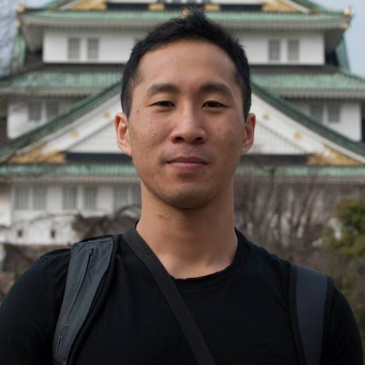
Paul L Tsang
age ~73
from Union City, CA
- Also known as:
-
- Paul Lukpong Tsang
- Paul T Tsang
- Paul L Ptsang
- Tsang Paul
- Phone and address:
-
4756 Loretta Way, Union City, CA 94587
(510)4895730
Paul Tsang Phones & Addresses
- 4756 Loretta Way, Union City, CA 94587 • (510)4895730 • (650)5933634
- 4755 Loretta Way, Union City, CA 94587
- San Carlos, CA
- San Jose, CA
- San Francisco, CA
- Foster City, CA
- Osceola, WI
Work
-
Company:Masterpiece portrait & wedding
-
Address:1160 El Camino Real, San Carlos, CA 94070
-
Phones:(650)5933634
-
Position:Owner
-
Industries:Photographic Studios, Portrait
Name / Title
Company / Classification
Phones & Addresses
Abbey Dental Centre
Dentists-General Practice
Dentists-General Practice
122 31935 S Fraser Way, Clearbrook, BC V2T 1V5
(604)8500768
(604)8500768
Owner
Masterpiece Portrait & Wedding
Photographic Studios, Portrait
Photographic Studios, Portrait
1160 El Camino Real, San Carlos, CA 94070
Website: mpwweb.com
Website: mpwweb.com
Owner
Masterpiece Portrait & Wedd
Photographic Studios, Portrait
Photographic Studios, Portrait
876 Laurel St, San Carlos, CA 94070
Website: aboutmasterpiece.com
Website: aboutmasterpiece.com
Owner
Masterpiece Portrait & Wedding
Photographers-Portrait
Photographers-Portrait
1160 El Camino Real, San Carlos, CA 94070
(650)5933634
(650)5933634
Treas
WELLS FARGO FLEET SERVICES, INC
C/O 4824 Park Gln Rd, Minneapolis, MN 55416
633 Folsom St, San Francisco, CA 94107
75 Pinehurst Way, San Francisco, CA 94117
633 Folsom St, San Francisco, CA 94107
75 Pinehurst Way, San Francisco, CA 94117
Mubeauty LLC
Retail and Wholesale and Online Sales of · Business Services at Non-Commercial Site · Nonclassifiable Establishments
Retail and Wholesale and Online Sales of · Business Services at Non-Commercial Site · Nonclassifiable Establishments
345 Capricorn Ave, Oakland, CA 94611
Abbey Dental Centre
Dentists-General Practice
Dentists-General Practice
(604)8500768
President
Hogan & Jones Chicken Inc
Us Patents
-
Method For Manufacturing Field Effect Transistors
view source -
US Patent:44425899, Apr 17, 1984
-
Filed:Mar 5, 1981
-
Appl. No.:6/240677
-
Inventors:Ven Y. Doo - San Jose CA
Paul J. Tsang - Poughkeepsie NY -
Assignee:International Business Machines Corporation - Armonk NY
-
International Classification:H01L 21265
H01L 2128 -
US Classification:29571
-
Abstract:A transistor and method of forming the same are disclosed. A thick mesa of dielectric material is grown on a semiconductor substrate and two or more layers of polycrystalline silicon grown on the vertical sides of the mesa serve a masking function to define the gate region of the transistor with high accuracy. The mesa and the two or more polycrystalline layers remain in the final device.
-
Bipolar Transistor
view source -
US Patent:43921493, Jul 5, 1983
-
Filed:Jun 15, 1981
-
Appl. No.:6/273705
-
Inventors:Cheng T. Horng - San Jose CA
Robert O. Schwenker - San Jose CA
Paul J. Tsang - Poughkeepsie NY -
Assignee:International Business Machines Corporation - Armonk NY
-
International Classification:H01L 2712
-
US Classification:357 49
-
Abstract:Disclosed is a self-aligned process for providing an improved bipolar transistor structure. The process includes the chemically etching of an intermediate insulating layer to undercut another top layer of a different insulating material in a self-aligned emitter process wherein the spacing of the emitter contact to the polysilicon base contact is reduced to a magnitude of approximately 0. 2 to 0. 3 micrometers. In addition, in the process an emitter plug is formed to block the emitter region from the heavy P+ ion dose implant of the extrinsic base.
-
Process For Fabricating Improved Bipolar Transistor Utilizing Selective Etching
view source -
US Patent:43098126, Jan 12, 1982
-
Filed:Mar 3, 1980
-
Appl. No.:6/126610
-
Inventors:Cheng T. Horng - San Jose CA
Robert O. Schwenker - San Jose CA
Paul J. Tsang - Poughkeepsie NY -
Assignee:International Business Machines Corporation - Armonk NY
-
International Classification:H01L 21265
H01L 21285
H01L 2131 -
US Classification:29578
-
Abstract:Disclosed is a self-aligned process for providing an improved bipolar transistor structure. The process includes the chemically etching of an intermediate insulating layer to undercut another top layer of a different insulating material in a self-aligned emitter process wherein the spacing of the emitter contact to the polysilicon base contact is reduced to a magnitude of approximately 0. 2 to 0. 3 micrometers. In addition, in the process an emitter plug is formed to block the emitter region from the heavy P+ ion dose implant of the extrinsic base.
Classmates

Alberta College, Edmonton...
view sourceGraduates:
Peter Tsang (1969-1973),
Dave Ottley (1964-1968),
Troy Weeks (1990-1992),
Paul Tsang Hong Yue (1967-1971),
Allan Campiou (1995-1999)
Dave Ottley (1964-1968),
Troy Weeks (1990-1992),
Paul Tsang Hong Yue (1967-1971),
Allan Campiou (1995-1999)

Hoover Middle School, San...
view sourceGraduates:
Paul Nathan (1952-1956),
Larry Minney (1956-1960),
Matthew Cogley (1987-1990),
Paul Tsang (1983-1987),
Hei Man Li (1999-2003)
Larry Minney (1956-1960),
Matthew Cogley (1987-1990),
Paul Tsang (1983-1987),
Hei Man Li (1999-2003)

Paul Tsang
view source
Paul Tsang
view source
Paul Tsang
view source
Paul C Tsang
view source
Paul Tsang
view source
Paul Tsang
view source
Paul Tsang
view source
Paul Tsang
view sourceMyspace
Youtube
Googleplus

Paul Tsang
Work:
Biglight - Designer
ACHICA - Graphic designer (2010-2013)
ACHICA - Graphic designer (2010-2013)

Paul Tsang
Education:
Leeds Metropolitan University - BSc Information System

Paul Tsang

Paul Tsang

Paul Tsang

Paul Tsang

Paul Tsang

Paul Tsang
Flickr
Get Report for Paul L Tsang from Union City, CA, age ~73


