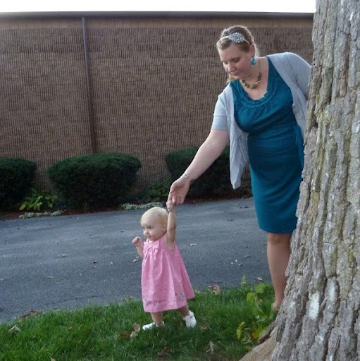
Sarah M Schwab
age ~39
from Newark, OH
- Also known as:
-
- Sarah E Schwab
- Sarah E Matesich
Sarah Schwab Phones & Addresses
- Newark, OH
- 110 Sandpiper Dr, Thornville, OH 43076 • (740)2422192
- Columbus, OH
- Dallas, TX
- Springfield, OH
- Granville, OH
- 816 Pavillion St, Dallas, TX 75204 • (214)8210633
Resumes

Sarah Schwab
view source
Sarah Schwab
view source
Sarah Schwab
view source
Sarah Schwab
view sourceLocation:
United States
Us Patents
-
Wafer-Scale Package For Surface Acoustic Wave Circuit And Method Of Manufacturing The Same
view source -
US Patent:6744336, Jun 1, 2004
-
Filed:Oct 15, 2002
-
Appl. No.:10/271392
-
Inventors:Martin Goetz - Dallas TX
Sarah Schwab - Dallas TX -
Assignee:Clarisay, Incorporated - Dallas TX
-
International Classification:H03H 964
-
US Classification:333193, 333195, 310313 B, 29 2535
-
Abstract:A surface acoustic wave (SAW) circuit package and a method of fabricating the package. In one embodiment, the package includes: (1) a substantially planar piezoelectric substrate, (2) SAW circuit conductors located over the substrate and (3) a passivation layer located over the SAW circuit conductors, the substrate and the passivation layer cooperating to form a hermetic seal to isolate the SAW circuit conductors from an environment proximate the package.
-
Wafer-Scale Package For Surface Acoustic Wave Circuit And Method Of Manufacturing The Same
view source -
US Patent:20020140525, Oct 3, 2002
-
Filed:Mar 29, 2001
-
Appl. No.:09/821592
-
Inventors:Martin Goetz - Dallas TX, US
Sarah Schwab - Dallas TX, US -
International Classification:H03H009/64
-
US Classification:333/193000, 310/31300R
-
Abstract:A surface acoustic wave (SAW) circuit package and a method of fabricating the package. In one embodiment, the package includes: (1) a substantially planar piezoelectric substrate, (2) SAW circuit conductors located over the substrate and (3) a passivation layer located over the SAW circuit conductors, the substrate and the passivation layer cooperating to form a hermetic seal to isolate the SAW circuit conductors from an environment proximate the package.
Classmates

Sarah Conner (Schwab)
view sourceSchools:
Baptist Academy Indianapolis IN 1995-1999
Community:
Ron Britt

Sarah Schwab
view sourceSchools:
Star Valley High School Afton WY 1997-2001
Community:
Robert Hunsaker

Sarah Schwab (Ganzen)
view sourceSchools:
Appleton North High School Appleton WI 1994-1998

Sarah Schwab (Wiesner)
view sourceSchools:
Beth Jacob-Bais Yaakov High School Brooklyn NY 1965-1969
Community:
Malkie Herskovits

Sarah Schwab (Herbertson)
view sourceSchools:
Cottingham Public School Toronto Morocco 1977-1984, Jesse Ketchum Elementary School Toronto Morocco 1984-1986
Community:
Gabe Nemeth, Joyce Reeves, Edward Collins, Gordon Postill

Sarah Duncan (Schwab)
view sourceSchools:
Vinita High School Vinita OK 2003-2007
Community:
Andrew Hillger, Stephanie Jackson, Jennifer Goforth, Felicia Hayes, Megan Greenwalt, Daniel Garrett, Martin Honeywell, Donnie Copeland, Toni Spaulding, Joe Doe, Sabrina Hayes

Sarah Christensen (Schwab)
view sourceSchools:
Fairfield High School Fairfield MT 1990-1994
Community:
Marie Hollo, Virginia Graves, Debbie Scott

Sarah Christensen (Schwab)
view sourceSchools:
Fairfield High School Fairfield MT 1990-1994
Community:
Marie Hollo, Virginia Graves, Debbie Scott

Sarah Schwab
view source
Sarah Schwab Ganzen
view source
Sarah Schwab
view source
Sarah Carter Schwab
view source
Sarah Vosler Schwab
view source
Sarah Thompson Schwab
view source
Sarah Lee Schwab
view source
Sarah Schwab Banks
view sourceMyspace
Youtube
Googleplus

Sarah Schwab
Work:
Headliners Hair Salon
Education:
Alpena Community College - Cosmetolgy

Sarah Schwab (Makeupbysar...
Tagline:
MakeUpBySarahSparkle: Affordable Makeup, Style, Beauty, & Fashion

Sarah Schwab

Sarah Schwab

Sarah Schwab

Sarah Schwab

Sarah Schwab

Sarah Schwab
Flickr
Get Report for Sarah M Schwab from Newark, OH, age ~39


